For years, researchers studying ultra-thin materials hit a frustrating wall: some of the most promising substances for future electronics were literally invisible under standard microscopes. Boron nitride, a single-atom-thick material sometimes called "white graphene," was transparent to visible light — which meant scientists couldn't actually see what they were building with it.
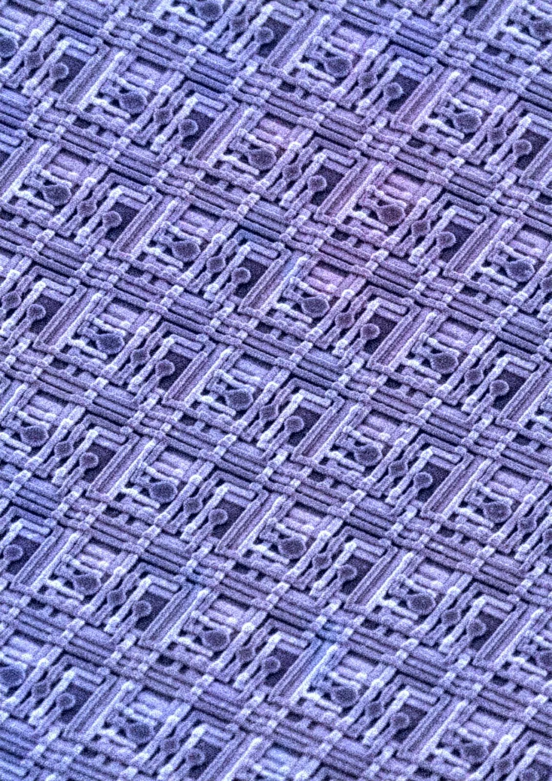
Now a team at Berlin's Fritz Haber Institute has solved that problem with an elegant trick. By mixing two laser beams — one in the infrared range and one in visible light — they've created a microscope that makes boron nitride glow. The technique, called phase-resolved sum-frequency microscopy, works by resonantly driving a vibration in the material's lattice, producing a bright signal that reveals not just the material itself, but also its crystal orientation.
Why this matters for the future
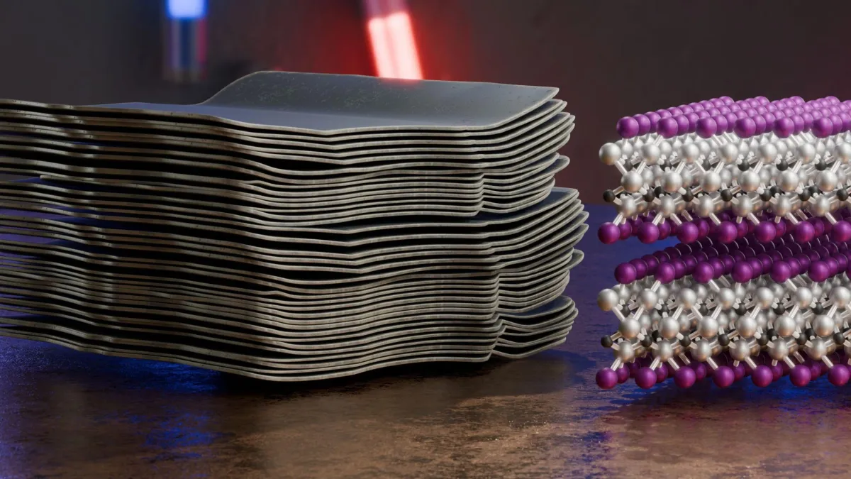
Two-dimensional materials — substances made from a single layer of atoms — are reshaping how scientists think about electronics and optics. Since graphene's discovery in 2004, researchers have created dozens of these atom-thin layers, each with unusual properties that bulk materials don't have. Boron nitride is already used in quantum optics and infrared technology, but only if researchers can see what they're doing.
We're a new kind of news feed.
Regular news is designed to drain you. We're a non-profit built to restore you. Every story we publish is scored for impact, progress, and hope.
Start Your News DetoxThe real promise lies in stacking these layers. When you place different 2D materials on top of each other in precise arrangements — what physicists call van der Waals structures — they can develop entirely new properties. But building these structures blindly is like assembling furniture in the dark. You need to see the orientation of each layer, spot any distortions or grain boundaries, and verify your work as you go.
The new microscope does all of this. It can image a 100 by 100 micrometer sample area in less than a second, producing images with far higher contrast than older atomic force microscopy methods. More importantly, it works as a live imaging tool — researchers can watch their layers stack and orient themselves in real time.
The Fritz Haber team discovered something else in the process: boron nitride's strong response at the vibrational resonance frequency makes it a promising candidate for frequency upconversion, converting infrared light into visible light in future optoelectronic devices.
The microscope isn't limited to boron nitride. The researchers anticipate using this imaging approach on a wider range of stacked 2D materials and their combinations, opening doors to materials science applications that were previously out of reach. The technique is non-invasive and requires no labels or dyes — just light and the material itself.