
Imagine trying to paint a detailed mural, but your only option is to slather paint everywhere and then painstakingly scrape away 90% of it. That’s essentially how we’ve been making patterns with carbon nanotubes — those tiny, incredibly strong materials crucial for advanced sensors and next-gen electronics.
Turns out, there’s a much smarter way. Researchers have developed a new, single-step process that patterns these valuable nanotubes with almost zero waste, saving both time and money. It’s the kind of innovation that makes you wonder why no one thought of it sooner.
Printing, But Smarter
The old method involved laying down a continuous film of expensive nanotubes, then etching away what wasn’t needed. Not only was this incredibly wasteful (up to 90% of the material gone!), but it also degraded the quality of the remaining nanotubes. Dmitry Krasnikov, a professor at Skoltech Photonics, describes single-walled carbon nanotubes as having "amazing properties for electronics and optics," so wasting them felt like a minor tragedy.
We're a new kind of news feed.
Regular news is designed to drain you. We're a non-profit built to restore you. Every story we publish is scored for impact, progress, and hope.
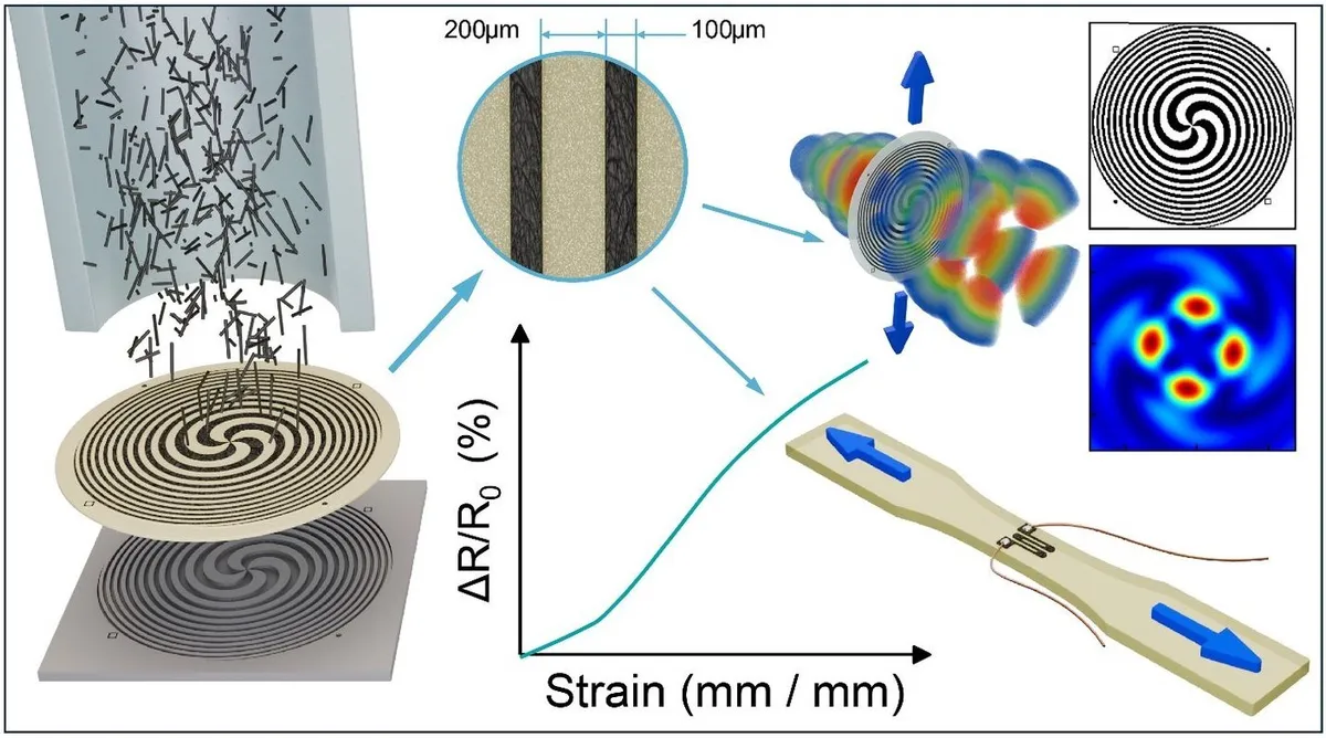
Start Your News DetoxThe new solution? A reusable stencil made from a common filter material called nitrocellulose. The team essentially uses a hot metal stencil, pressed at about 200 megapascals (that’s 2,000 times atmospheric pressure, for context), to clog the pores in the filter where nanotubes aren't wanted. Think of it as creating a very precise, microscopic sieve.
When the nanotubes are then applied using aerosol chemical vapor deposition — a fancy way of saying they float through gas — they only pass through the open pores, creating the desired pattern directly. No etching, no solvents, no wasted material. Just clean, high-quality patterns. As Albert Nasibulin, who leads Skoltech Photonics, puts it, the nanotubes are so light they just follow the gas flow, and by closing off the unwanted pores, the gas itself does the patterning.
This isn't their first rodeo. An earlier version used copper to block pores, but that had its own issues, like limiting pattern types and leaving behind copper residue. The hot-pressing technique eliminates those problems entirely, allowing for intricate designs without compromising the nanotubes' integrity.
Wearables and Wireless, With Nanotubes
The team didn't just stop at a clever new method; they immediately put it to work. Nikita Raginov, the lead author, highlighted the method’s scalability for optics, electronics, and sensing. They created two devices that showcase the tech's potential:
- A mechanical strain sensor: This W-shaped nanotube pattern on an epoxy base changes electrical conductivity when stretched. It’s at least three times more sensitive than similar sensors made with older methods, and it remained stable over 3,000 stretch-and-relax cycles. Imagine this in aircraft wings, bridge pillars, or even your next smart shirt, constantly monitoring structural health or your body’s movements.
- A tunable terahertz lens: A spiral nanotube structure on a stretchy film created a flexible lens that can focus terahertz waves (the sweet spot between infrared and microwaves). The best part? You can change its focal distance by simply stretching it. This could be a game-changer for wireless communication and data transmission, allowing for dynamic control over how information is sent.
Beyond these, the researchers envision applications in transparent conductors, bioelectrodes, and even heating grids. It's a reminder that sometimes, the most elegant solutions are the ones that simply stop making a mess in the first place.