A team of scientists found a crystal that can be changed and programmed using regular light. This discovery could help build new optical technology.
Researchers at the XPANCEO Emerging Technologies Research Center, with Nobel Laureate Prof. Konstantin Novoselov, found unusual optical behavior in arsenic trisulfide (As2S3). This material is a crystalline van der Waals semiconductor.
Their work shows that light can permanently change this material. It can even be shaped at a tiny scale using simple continuous-wave (CW) light. This means expensive cleanroom tools or advanced laser systems are not needed.
We're a new kind of news feed.
Regular news is designed to drain you. We're a non-profit built to restore you. Every story we publish is scored for impact, progress, and hope.
Start Your News DetoxHow Light Changes the Crystal
The discovery relies on a property called the refractive index. This property shows how much a material bends or slows light. Materials with a higher refractive index are better at guiding light. Sometimes, light itself can change this property. This is called photorefractivity.
Crystalline As2S3 shows this effect even with low-intensity ultraviolet light. The material's refractive index changed a lot when exposed to light, up to Δn ≈ 0.3. This change is much bigger than what is usually seen in other photorefractive materials like BaTiO3 or LiNbO3.
Writing Optical Functions with Light
Materials with strong photorefractive responses allow optical functions to be created directly inside them using light. Instead of complex manufacturing, light can define how the material interacts with optical signals.
This ability has many uses. It can form tiny structures that guide light in telecommunications. It can also create diffractive elements for sensors and imaging. Additionally, it can produce hologram-like features for security, where the optical pattern acts as a unique identifier.
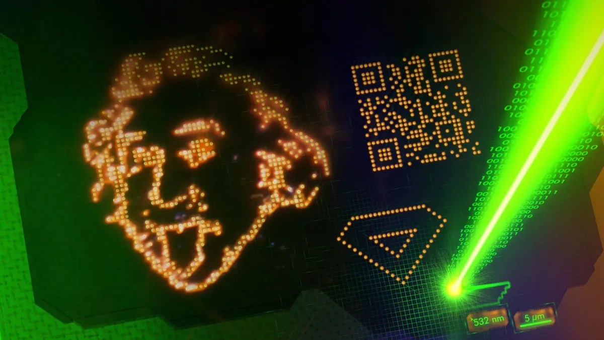
Nanoscale Patterns and Optical Fingerprints
These effects work at very small scales in As2S3. The big change in refractive index allows for detailed patterns to be made inside the transparent material. These patterns can be like "optical fingerprints" that are hard to copy. This makes them useful for fighting fake products and tracking items.
To show this control, researchers used a standard laser to "sculpt" a tiny portrait of Albert Einstein on a thin piece of the material. The points were 700 nanometers apart. Other tests showed even higher detail, down to 500 nanometers between points. The patterns are very clear because of the light-induced refractive index change.
Valentyn Volkov, Founder and Chief Technology Officer at XPANCEO, said that finding new functional materials, especially van der Waals crystals, is key for photonics. He noted that developing complex optical devices, like smart contact lenses, needs a strong base in materials science. He added that identifying natural crystals with this sensitivity provides the building blocks for new light-driven technology.
Expanding Crystals for New Devices
Besides changing its optical properties, As2S3 also expands physically when exposed to light. The material can grow up to 5%. This allows researchers to directly create structures like microlenses and gratings on its surface.
These features are important for making wide field-of-view waveguides used in augmented reality glasses and smart contact lenses. The material's sensitivity also makes it good for photonic circuits and tiny sensors. These properties are a big step forward in controlling light for future technologies.
Deep Dive & References
Giant photorefractive and photoexpansion effects in a van der Waals semiconductor - Proceedings of the National Academy of Sciences, 2026