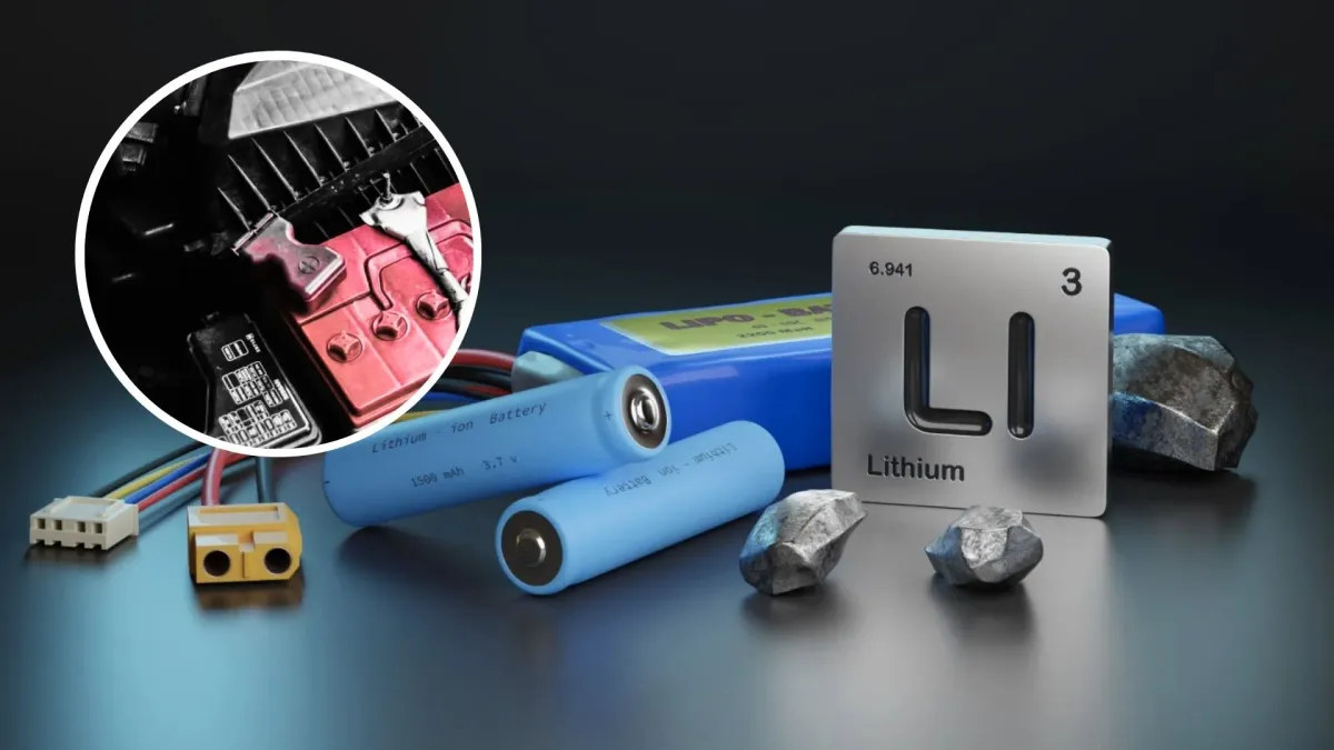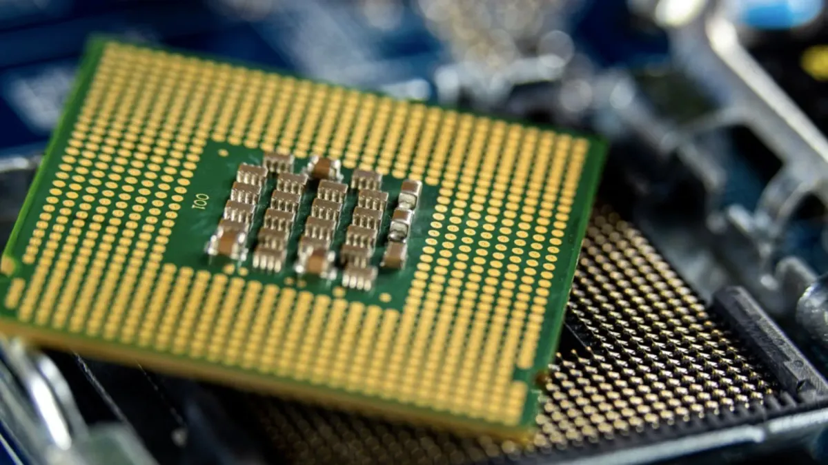
China's semiconductor scene is heating up, and not just in the usual ways. Chip firm JCET is dropping a cool $1.15 billion on a new manufacturing plant in Shanghai. Why? Because apparently, the final frontier of chipmaking is where all the action is now, especially with AI demanding more processing power than ever before.
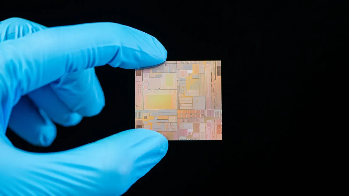
This isn't just any old factory. It's all about advanced chip packaging and testing – the delicate art of turning individual chip parts into finished, functional products. Think of it as the grand finale of semiconductor production, and China wants to own the stage.

The Endgame of Chip Production
JCET, already a big name in the packaging and testing game, is funneling this massive investment through a subsidiary with a hefty $560 million in registered capital. The new facility will call Shanghai’s Lingang Special Area home, which sounds appropriately futuristic for a project of this scale.
We're a new kind of news feed.
Regular news is designed to drain you. We're a non-profit built to restore you. Every story we publish is scored for impact, progress, and hope.
Start Your News DetoxThe whole endeavor is a two-act play, with the curtain rising on construction and equipment installation by the second half of 2028. Because if you're going to boost your high-end packaging capabilities and solidify your market position, you might as well take your time and do it right.
This push for self-sufficiency has become particularly urgent thanks to U.S. export restrictions, which have made access to top-tier chip manufacturers like TSMC a bit, shall we say, complicated. So, China is doing what any determined nation would: building its own.

And investors? They're loving it. JCET's shares in Shanghai have shot up 147% since the beginning of the year. Because nothing says "we're serious" like a multi-billion dollar investment and a skyrocketing stock price.
The Post-Moore's Law Era
According to JCET’s CEO, Zheng Li, we're officially in a "post-Moore’s Law" era. For decades, chip improvements were all about shrinking transistors. Now, that's getting harder and more expensive than trying to fold a fitted sheet perfectly.
So, advanced packaging steps in as the new superhero. Instead of just making things smaller, it's about combining many tiny chips and designs into one super-powerful, energy-efficient system. Which, if you think about it, is both impressive and slightly terrifying for anyone who remembers when a computer took up a whole room.

Zheng noted that next-generation packaging methods are aiming to reduce surface roughness to less than 0.2 nanometers. That's a significant leap from the 5 nanometers seen in current 2.5D packaging technology. Imagine the precision required. It's like going from building with LEGOs to assembling a Swiss watch… blindfolded. But for AI. Because apparently, that's where we are now.