A team of researchers has built an AI system that can map out complex defect patterns in liquid crystals almost instantly—cutting simulation time from hours down to milliseconds. The breakthrough could reshape how scientists design and test advanced materials.
The work hinges on a simple but powerful idea: instead of running expensive computational simulations over and over, teach a neural network to recognize patterns in the data and predict outcomes directly.
Why Defects Matter
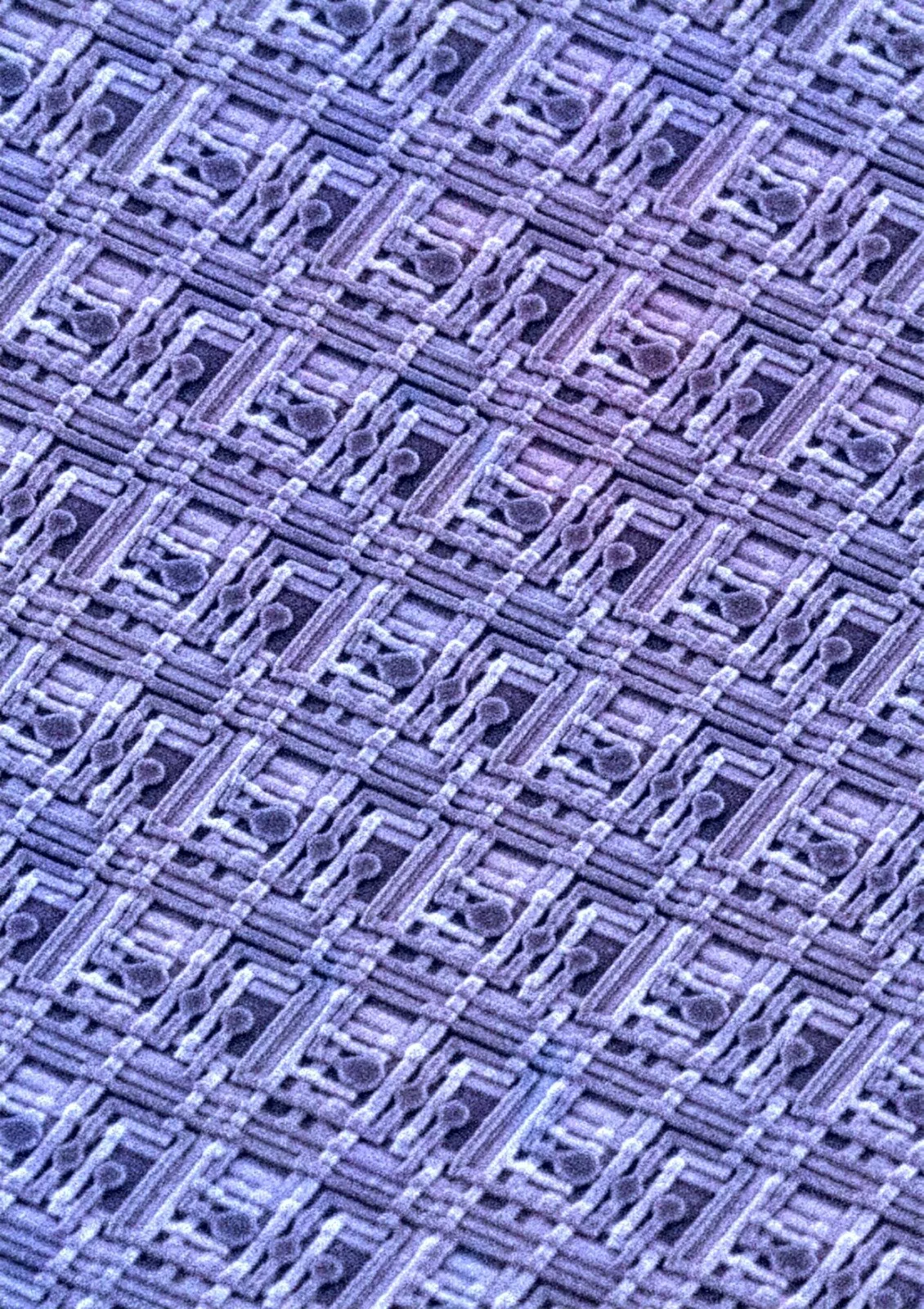
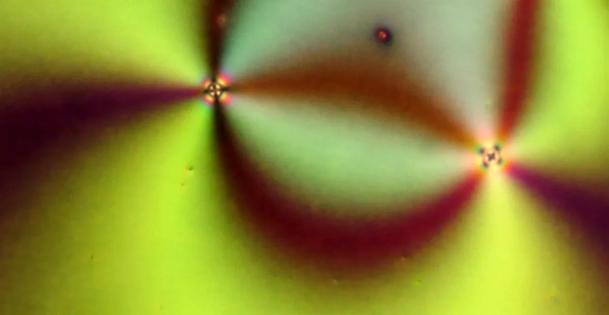
When physical systems shift from balanced to ordered states, tiny irregularities often appear. These "topological defects" show up everywhere—in the structure of the universe, in everyday materials, in the molecular arrangement of liquid crystals. Scientists study them because they reveal how order emerges from chaos, and because controlling defects is key to engineering better materials.
We're a new kind of news feed.
Regular news is designed to drain you. We're a non-profit built to restore you. Every story we publish is scored for impact, progress, and hope.
Start Your News DetoxLiquid crystals are especially useful for this work. The molecules can rotate freely while pointing roughly the same direction, making them a controllable lab for watching defects form and shift. Researchers usually describe these systems using Landau-de Gennes theory, a mathematical framework that explains how molecular order breaks down at defect cores.
But running these simulations is slow. Hours of computation for a single configuration.
The AI Shortcut
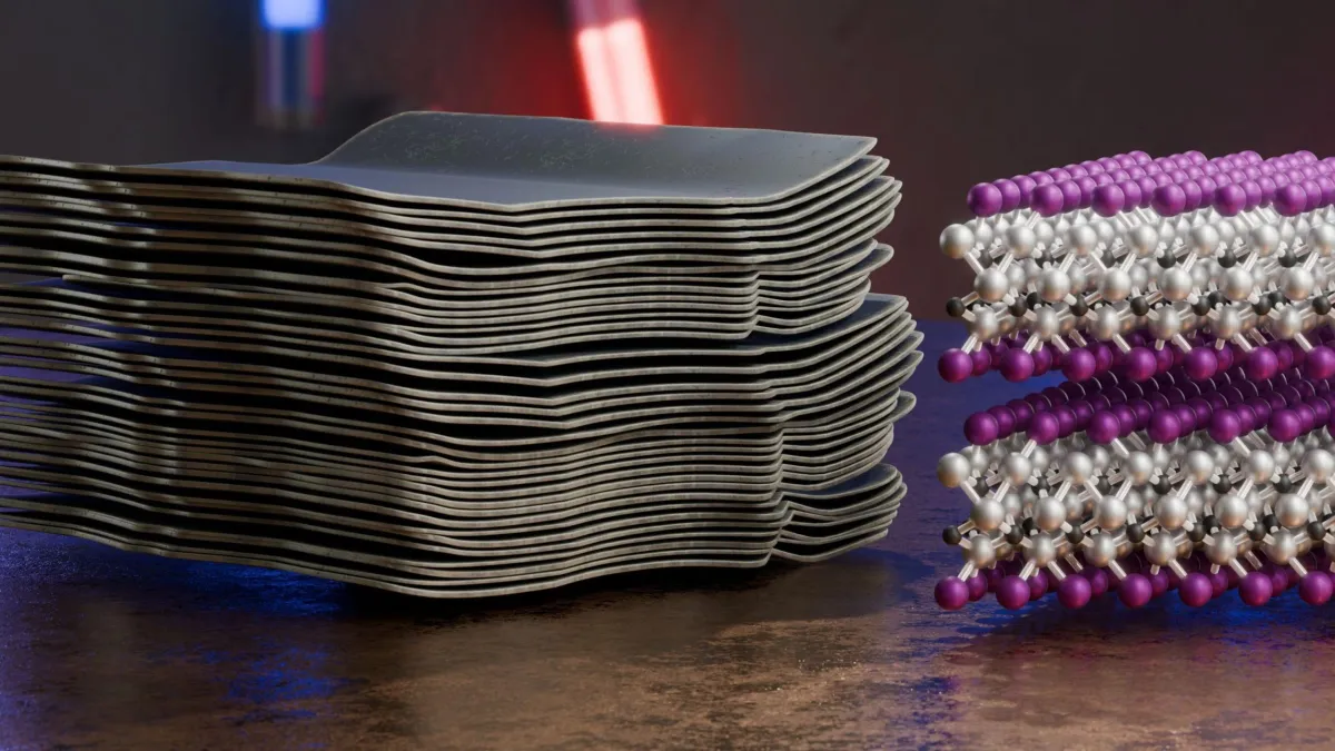
Professor Jun-Hee Na's team at Chungnam National University took a different path. They trained a deep learning model—specifically a 3D U-Net architecture, the kind often used in medical imaging—to learn the physics directly from data instead of calculating it from equations.
The system works like this: you feed it boundary conditions (how molecules align at the edges), and it predicts the full molecular alignment field across the entire space, including where defects appear and what shape they take. After training on conventional simulations spanning a wide range of patterns, the model could predict entirely new configurations it had never seen before. The results matched both traditional simulations and real experiments.
The speed gain is the real story here. What took hours now takes milliseconds. That's not just convenience—it's a fundamental shift in what's possible.
Opening New Design Possibilities
With this kind of speed, researchers can now explore vast design spaces quickly, testing thousands of material configurations to find ones with precisely controlled defect structures. That matters for optical devices, metamaterials, and smart surfaces that need to behave in specific ways.
"By drastically shortening the material development process, AI-driven design could accelerate the creation of smart materials for applications ranging from holographic displays to adaptive optical systems and smart windows," Na says.
The model handles complex scenarios too—including higher-order defects that merge, divide, or rearrange. Experiments confirmed it reproduces these behaviors reliably across different conditions.
This is the kind of work that quietly reshapes how science happens. Not a single breakthrough material, but a tool that makes the next hundred breakthroughs faster to find.