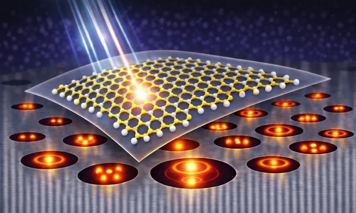
Tungsten disulfide is just one atom thick, yet researchers have found a way to make it interact with light about twenty times more intensely than before. The trick wasn't to change the material itself—it was to reshape the empty space beneath it.
Atomically thin semiconductors have become the darlings of nanophotonics because they can produce new colors of light and capture light signals with remarkable efficiency, despite being impossibly small. But there's a catch: when you have only a single layer of atoms, light doesn't spend much time interacting with it. It's like trying to have a conversation with someone walking past—the interaction is brief and weak unless you find a way to slow them down.
Researchers at the Max Planck Institute (and collaborators published in Advanced Photonics) found that solution by creating a hybrid structure: they etched nanoscale air cavities—called Mie voids—into a crystal of bismuth telluride, then placed a monolayer of tungsten disulfide on top. The air pockets act like tiny mirrors, bouncing light back and forth in precisely the right way to concentrate it exactly where the atomically thin layer can grab it.
We're a new kind of news feed.
Regular news is designed to drain you. We're a non-profit built to restore you. Every story we publish is scored for impact, progress, and hope.
Start Your News DetoxWhy air beats solid material
Traditional nanophotonic designs trap light inside solid structures like silicon. That works, but it concentrates the optical field deep within the bulk material, away from the surface where atomically thin layers live. It's like trying to warm your hands by putting them inside a solid block rather than near a fire.
Mie voids flip this logic. Instead of confining light inside a dense material, they confine it within tiny air gaps. The high refractive index of bismuth telluride creates strong reflections at the air-crystal boundary, keeping light bouncing inside the cavity. The optical field concentrates in the air itself—right at the surface where the tungsten disulfide sits. This design also works even when the host material absorbs light strongly, which would normally ruin conventional resonators.
The researchers engineered the cavities by ion-beam milling and tuned them so their resonant wavelength matched the primary light-emission feature of tungsten disulfide. When they measured the light emitted from the monolayer, they found a roughly twentyfold increase in intensity when the cavity resonance overlapped with the emission band. They also tested frequency conversion—when they shifted the cavities to the near-infrared range, the second-harmonic signal jumped by about twenty-five times compared with non-resonant cavities.
What makes this approach particularly elegant is that it reveals something counterintuitive about nanoscale physics: shaping the empty space around a material can be just as powerful as choosing the right material in the first place. The air cavities don't just amplify signals—they also allow researchers to directly image the optical fields dancing across individual voids, turning invisible light patterns into visible hotspots that shift predictably as cavity geometry changes.
What this opens up
This platform could accelerate development in quantum optics, on-chip light sources, and sensing applications where weak signals are the limiting factor. Because the design works with materials that normally absorb light too strongly for conventional devices, it expands the toolkit of what's possible in two-dimensional semiconductors. The next phase will likely involve integrating these Mie-void structures with other van der Waals materials and exploring whether the same principle can enhance other light-matter interactions that have remained stubbornly weak at the atomic scale.