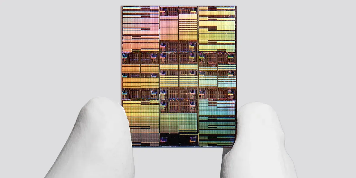
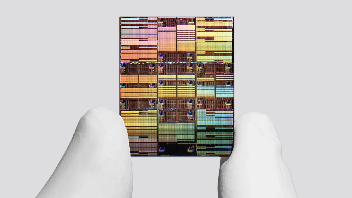
IBM has created a new prototype chip that packs about 100 billion transistors onto a space the size of a fingernail. This is twice as dense as their previous top technology from 2021. This new design could lead to faster, more energy-efficient computers for years to come.
For over 50 years, chipmakers have made computers more powerful by following Moore's Law. This means fitting more transistors onto a chip. Transistors are tiny switches that do calculations. They have been shrinking to smaller sizes. However, in the last 15 years, transistors have gotten so small that quantum mechanics starts to affect how they work. They are now only a few dozen nanometers in size and cannot get much smaller.
Building Up, Not Just Out
To fit more transistors, engineers are now looking at stacking them vertically, much like urban planners build taller buildings. IBM announced it has created a chip using this method. This new design, called a nanostack, places transistors in two layers on a silicon chip.
We're a new kind of news feed.
Regular news is designed to drain you. We're a non-profit built to restore you. Every story we publish is scored for impact, progress, and hope.
Start Your News DetoxJay Gambetta, director of IBM Research, called this a "meaningful leap forward." He expects nanostacking chips to be common in data centers within a decade. Their improved efficiency could help data centers use less energy.
Dan Hutcheson, vice chair of TechInsights, agrees. He says this technology is "transformational" and could extend the roadmap for chip development by another 10 to 15 years.
IBM reports that chips made with this new method can do 50% more work in the same time. They can also be up to 70% more energy efficient compared to IBM's previous best architecture.
This architecture provides a general way to arrange transistors. IBM plans to work with semiconductor manufacturers to make the actual chips. They expect chip designers to use this design in many types of chips, including GPUs and CPUs. Huiming Bu, IBM’s vice president of global semiconductor R&D, looks forward to discussing how designers can use this technology.
How the "Layer Cake" Chip is Made
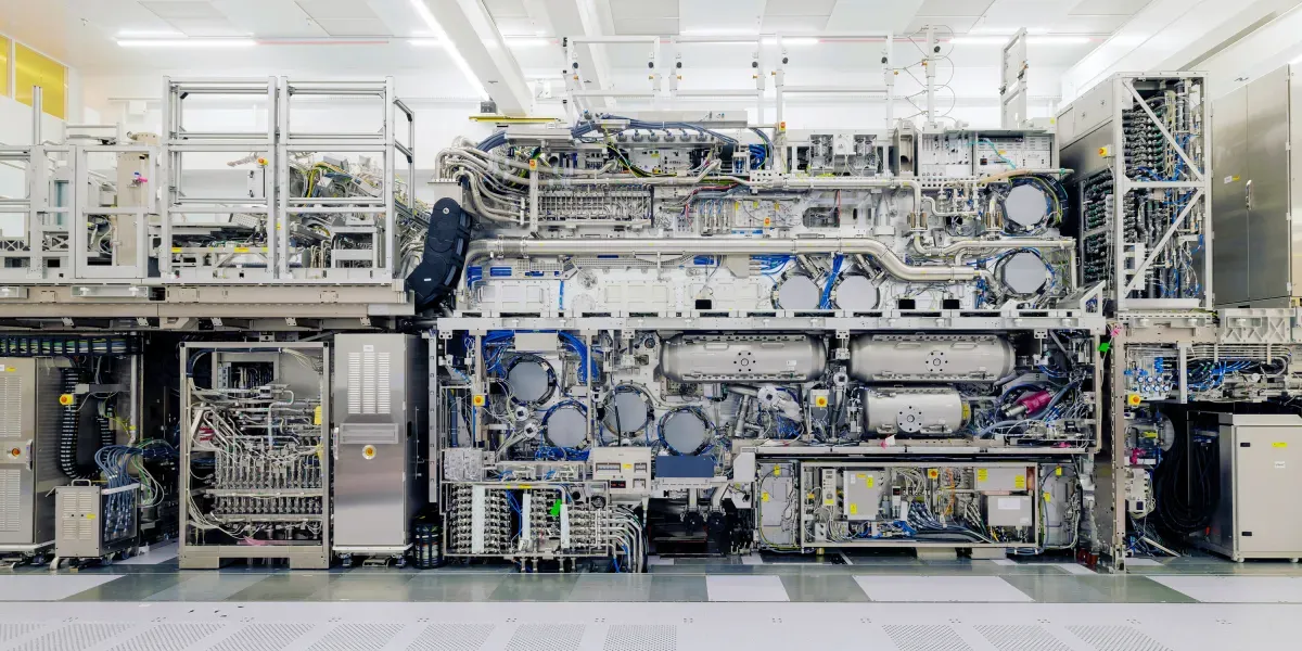
Engineers built IBM's new chip layer by layer, like a cake. First, they make transistors on one silicon layer. Then, they put another silicon layer on top and make more transistors directly on that. Finally, they create the electrical connections between the two layers.
This vertical stacking, which combines two types of transistors, is called a complementary field-effect transistor, or CFET. Qing Cao, a professor at the University of Illinois at Urbana-Champaign, explained this. He was not involved in IBM's work.
IBM is not the only company exploring this approach. Major chipmakers like Intel, Samsung, and TSMC, along with research lab Imec, are also researching CFETs. IBM says its design is unique because the second layer of transistors is staggered, not directly on top of the first. This makes wiring simpler, among other benefits.
CFETs, like those in IBM's nanostack, differ from other two-tiered chip methods. For example, AMD's 3D V-Cache and Huawei's upcoming LogicFolding technology make transistors on each layer separately and then bond them together. IBM's new method allows for more precise alignment of layers, which is crucial for performance due to the tiny size of transistors, Cao noted.
Nanostacking builds on a method called the nanosheet, used in current advanced transistors since about 2022. A transistor acts like a hose for electrons, with a valve to turn the flow on or off. Electrons move through a silicon patch called a channel. In IBM's nanostack, the channel has three nanosheets, each 15 atoms thick and nine nanometers apart.
IBM calls its nanostack technology "sub-nanometer" or "0.7 nanometer" node. This follows an industry tradition of naming generations after smaller lengths. However, "0.7 nanometer" is a marketing term and doesn't reflect a physical size on the chip. Cao points out that the distance between transistors has stayed around 40 nanometers for a long time.
Challenges in Production
Looking ahead, chipmakers could try to increase transistor density by adding more layers, as Bu suggested. However, this comes with practical challenges, according to Cao. Manufacturing always has errors, meaning some chips are faulty from the start. With multiple layers, if either the top or bottom layer fails, the whole chip fails. This higher failure rate would be costly compared to single-layer chips.
Another major challenge is the "thermal budget." Engineers must build each layer without melting the connections below it. This means keeping manufacturing processes below 400°C. IBM found a way to make the second stack at a low enough temperature, though they haven't shared their exact methods.
Academics are also working on this. Cao's group, for instance, developed a method to stack transistors layer by layer, similar to IBM, using processes below 200°C. They achieve this with junctionless transistors, which don't need a high-temperature step called doping. Doping injects non-silicon atoms into silicon to change its properties. Cao believes his approach could be easier to scale to multiple layers from a thermal management perspective, though it's currently a proof of concept.
Cao considers IBM's work "transformative" because it shows how to stack transistors "on a full wafer using a state-of-the-art manufacturing line." He says this new approach advances the industry, and he is eager to see its "killer application."