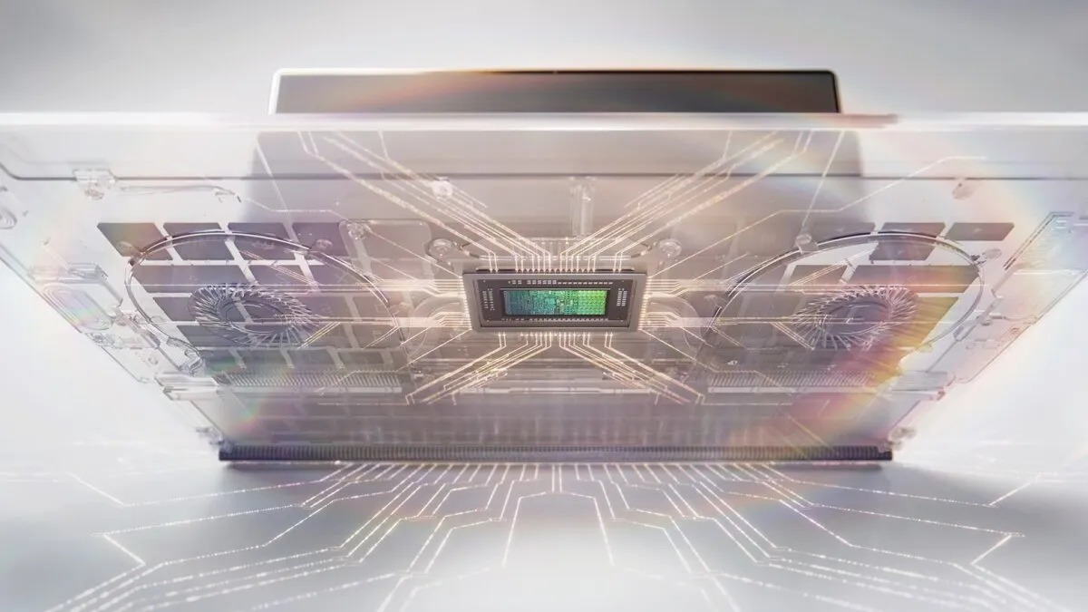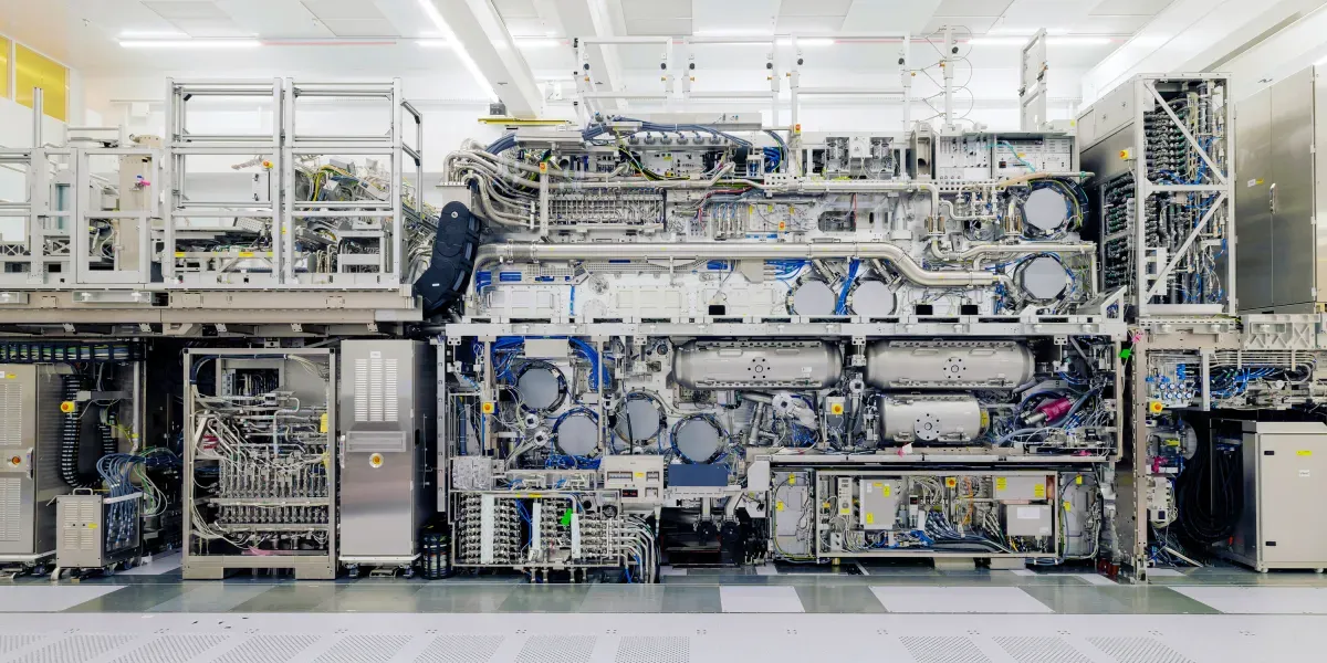
Imagine a machine the size of a double-decker bus, weighing over 150 tons, that costs more than a small country's annual budget. Now imagine it's the most important piece of tech you've never heard of, and it's currently being shipped to factories for a cool $400 million a pop. That's ASML's newest lithography tool, and it's basically the reason your AI models can do anything at all.
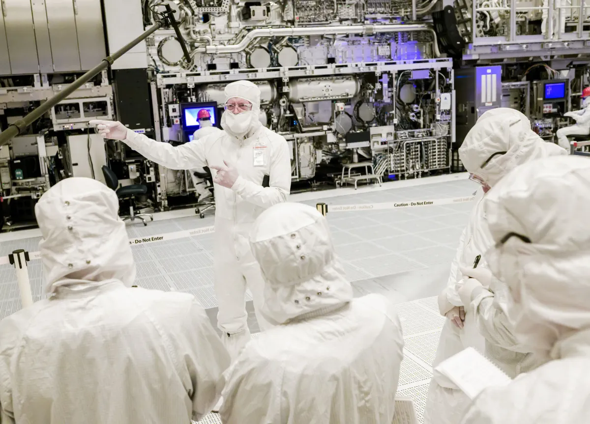
Jos Benschop, an ASML exec, has spent over a decade designing this beast. His company, a Dutch powerhouse, has a near-monopoly on the machines that use light to etch impossibly tiny circuits onto silicon wafers. These circuits become the transistors and wiring for every microchip that powers your phone, your car, and now, the burgeoning AI industry.
The Race for Tiny
Nine years ago, ASML rolled out machines using extreme-ultraviolet light (EUV), which created features as small as 13 nanometers. (For reference, a human hair is about 100,000 nanometers thick.) These new machines? They can hit a resolution of just eight nanometers – roughly the width of 40 silicon atoms. Let that satisfyingly tiny number sink in.
We're a new kind of news feed.
Regular news is designed to drain you. We're a non-profit built to restore you. Every story we publish is scored for impact, progress, and hope.
Start Your News Detox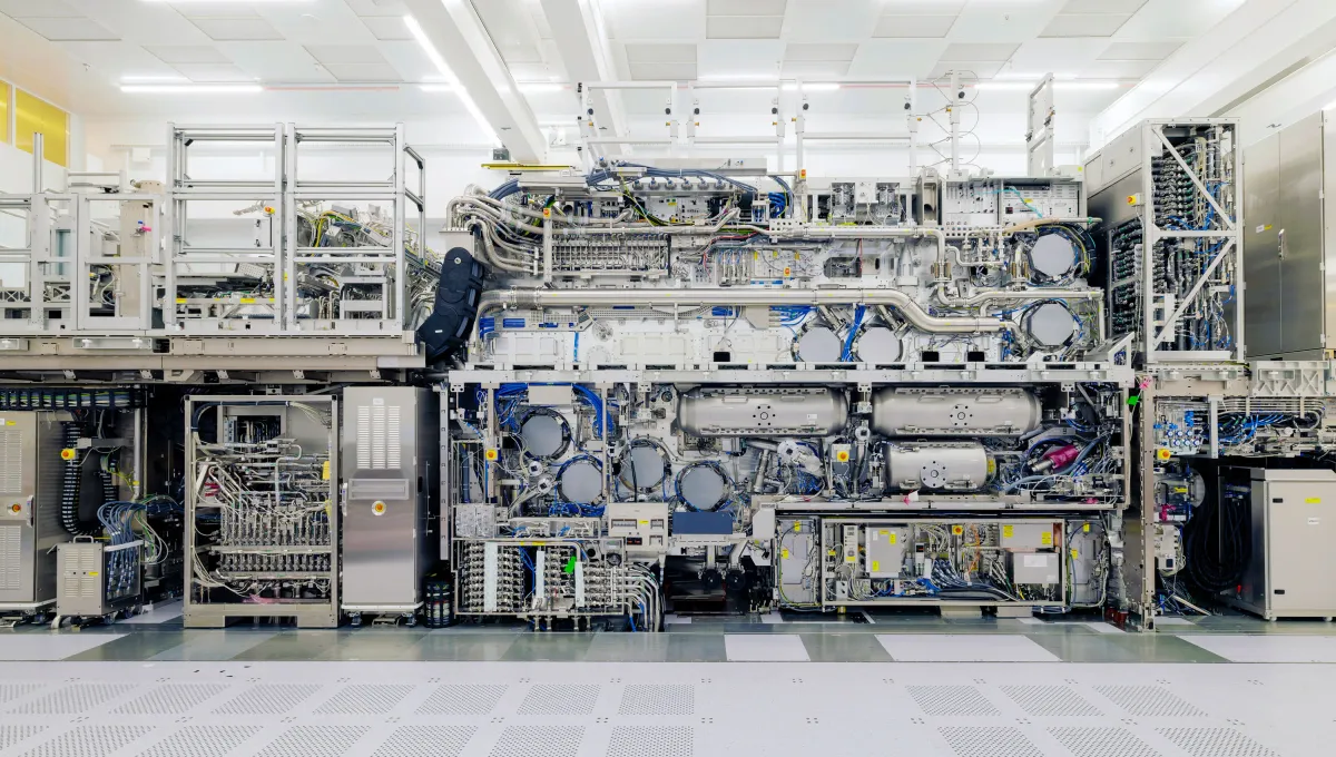
Chipmakers are shelling out $400 million each for these machines because the demand for faster, more energy-efficient chips is insatiable. The AI boom, driven by companies like OpenAI and Anthropic, has only amplified this. ASML's tools have been the unsung hero keeping Moore's Law — the prediction that chip density doubles every two years — alive and well.
Marco Pieters, ASML’s CTO, put it best: enabling smaller features opens up "mind-blowing" possibilities for AI, and we've only seen "the tip of the iceberg." Which, if you think about it, is both impressive and slightly terrifying.
ASML's dominance is undeniable, producing about 90% of all chip-lithography tools globally. This makes them, and Taiwan's TSMC (which uses ASML's machines to make most microchips), a powerful duopoly. So powerful, in fact, that it has governments a bit twitchy.
Chips as the New Oil
To curb China's advanced AI ambitions, the US pressured the Dutch government into an embargo in 2019, blocking ASML from selling high-end machines to Chinese firms. Marc Hijink, author of Focus: The ASML Way, calls chips "the new oil," and it's easy to see why. This geopolitical chess game has left some wondering if relying so heavily on one overseas, expensive supply chain is a good idea.
Naturally, competition is brewing. China is pouring billions into trying to replicate ASML's tech, and startups like Substrate are trying to build cheaper, smaller, and more capable machines. Because apparently, that's where we are now: tiny silicon wars.
The Evolution of Light (and Lots of Tin)
Making a chip is a bit like silk-screening a T-shirt, but with light, chemicals, and precision that would make a surgeon blush. The smaller the wavelength of light, the tinier the circuits you can etch. For decades, it was a two-step dance: find a new light source, then crank up its focusing power.
Back in the early 2000s, ASML, then a smaller fish, made a massive bet on EUV light. Everyone else, including giants like Nikon and Canon, eventually threw in the towel. EUV light is so finicky it's absorbed by glass and even air, requiring machines to operate in a vacuum. ASML expected it to take six years and $10 billion. It took 16 years and the same amount of money, but it worked.
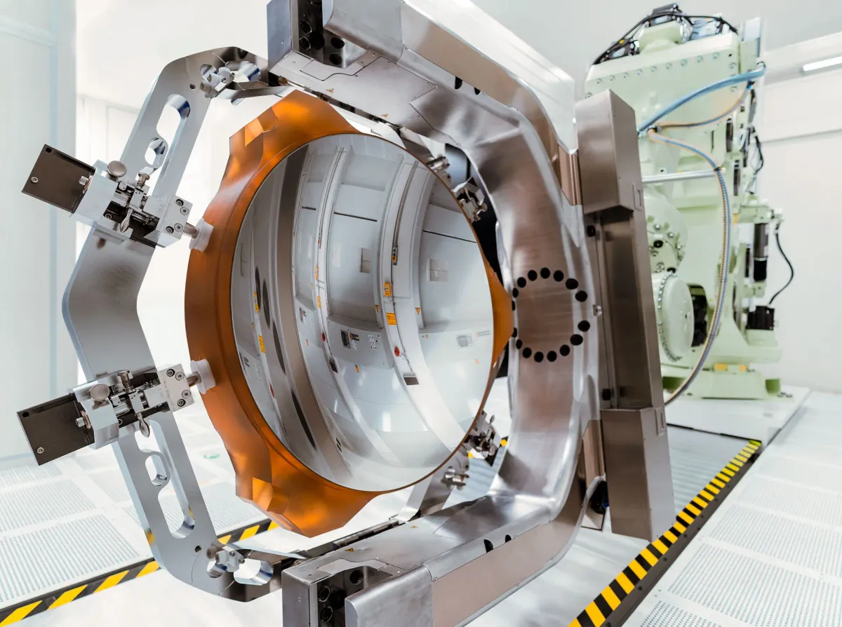
These machines create EUV light by vaporizing molten tin droplets with lasers, thousands of times a second. German optics company Zeiss developed mirrors polished with atomic precision to direct this light. Jeff Koch, an analyst and former ASML employee, noted that ASML "ignored the buzz of, like, Hey, this is never gonna work, and they just beat their heads against these huge engineering problems."
When the first EUV machines launched in 2017, they cost over $100 million. Some wondered if the demand would be there. Then OpenAI released GPT-3 and ChatGPT, and suddenly, everyone needed high-end chips yesterday. Nvidia's $40,000 AI training GPUs were flying off the shelves, and ASML's EUV machines made it easier and faster to produce them. The company's market value is now over half a trillion dollars. Not bad for betting on tin.
Intel's Big Bet and the Future of Tiny
Intel, eager to reclaim its silicon crown after losing ground in mobile and AI chips, was the first customer for ASML's new high-NA machines. In spring 2024, 300 ASML engineers descended on an Intel fab in Oregon to assemble and test the behemoth. Intel hopes being first to the high-NA party will give it an edge in its new foundry business, where it plans to manufacture chips for other companies, competing directly with TSMC.
High-NA also simplifies chip design. Previously, designers had to use "multi-patterning" — essentially blasting a wafer multiple times to create smaller features. High-NA allows "single patterning," making design much easier. TSMC, meanwhile, is playing it a bit cooler, waiting for high-NA to be "mature and ready" before diving in, perhaps wary of the $400 million price tag for what some see as an evolutionary, not revolutionary, leap.
But the story doesn't end with light. Startups like Substrate are developing tools using x-ray light from particle accelerators, aiming for even tinier features and cheaper production. And then there's Lace Lithography, a Norwegian startup, which is ditching light entirely for a beam of energized helium atoms. Their tools are much smaller, offer even greater precision, and require less power.
ASML's Benschop is watching, but he's not sweating it just yet. He believes ASML's EUV mastery will keep them ahead, seeing "no serious runner-up" for advanced chip manufacturing in the near future. ASML executives expect high-NA to dominate into the 2030s, with "hyper NA" (even higher numerical aperture) tools potentially arriving in the second half of that decade, pushing to a mind-bending six-nanometer resolution.
As Marco Pieters says, "We're pushing the limits of physics." The real question is, who can push harder? Because the race for tiny is only just beginning.