For decades, scientists have been scratching their heads over a class of materials called relaxor ferroelectrics. These aren't just fancy words; these materials are the unsung heroes behind your medical ultrasounds, the sonar pinging under ships, and a whole host of super-sensitive sensors. Problem was, their internal atomic structure was a jumbled mess, a secret even to the people who built things with them.
Now, a team from MIT and other institutions has finally pulled back the curtain, creating the first-ever 3D atomic charge map of these enigmatic substances. Think of it as finally getting a blueprint for a house where you only had vague sketches before.

Peeking Inside the Atomic Mess
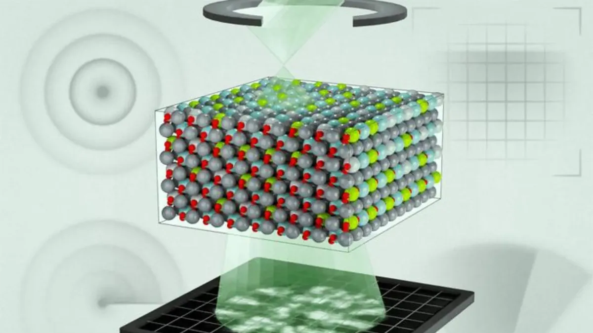
Relaxor ferroelectrics are known for being incredibly twitchy when an electric field comes calling. Unlike neat-freak crystals where atoms line up perfectly, relaxors are more like a teenager's bedroom: chemically disordered. This new map revealed that the internal charged areas, called polar regions, are far smaller and more intricate than any computer model had predicted.
We're a new kind of news feed.
Regular news is designed to drain you. We're a non-profit built to restore you. Every story we publish is scored for impact, progress, and hope.
Start Your News DetoxMIT professor James LeBeau put it plainly: understanding what's actually happening inside these materials means scientists can finally design them with specific superpowers in mind. Because, as he noted, "validating models is crucial for engineering these materials." No more guesswork, just highly informed design.
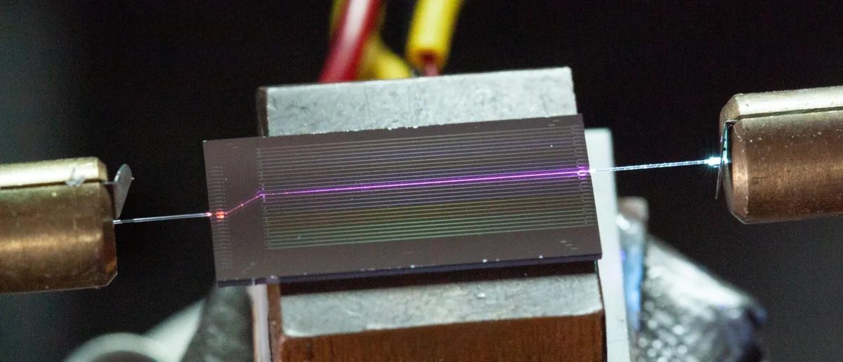
To pull off this atomic cartography, the researchers used a technique with a name that sounds like a secret government project: multi-slice electron ptychography. Essentially, they scanned a super-fine electron probe across the material, gathering overlapping patterns. Then, algorithms stitched these patterns together into a high-resolution 3D map. It's like scanning a QR code, but for individual atoms and their electric charges.

This method uncovered a level of "chemical disorder" that previous models completely missed. They could literally see tiny, previously invisible nanoregions within a specific alloy (lead magnesium niobate-lead titanate). This allowed them to map the internal interactions that give the material its incredible energy storage and sensing abilities. Until now, these details were pure speculation.
Building Better Everything
One of the big surprises? Many of those crucial "polar regions"—the pockets of charge that make the material tick—were much, much smaller than expected. Integrating this new, granular data into simulations instantly made those models more accurate, showing precisely how different chemicals and charge states play together to control the material's behavior.
LeBeau emphasized that as materials science gets more complex, fueled by AI and advanced computing, accurate models are absolutely non-negotiable. Otherwise, he warned, "the results will be flawed." This new technique ensures scientists know why materials behave the way they do, which is a pretty fundamental step toward making them behave even better.
With this "validated map" in hand, the discovery is poised to accelerate the creation of next-gen tech. We're talking more precise medical ultrasounds (finally, a clear picture of what's going on in there), sharper sonar systems, higher-capacity energy storage for all our gadgets, and advanced electronic components for computing that's even faster. Because apparently, that's where we are now. The findings, for those who like to check the footnotes, were published in Science.