Imagine trying to catch a wave in a puddle. Now imagine that puddle is 1,000 times thinner than one of your eyelashes, and the wave is light. That’s essentially what a team of Polish scientists just pulled off, trapping infrared light in a layer a mere 40 nanometers thick.
Because apparently that’s where we are now: making structures so impossibly small they make a human hair look like a redwood. This isn't just a parlor trick; it's a huge leap toward light-based technologies that are faster, tinier, and could make your current electronics look positively ancient.
The team, primarily from the University of Warsaw, published their findings in ACS Nano, detailing how they bent light to their will in ways previously thought impossible.
We're a new kind of news feed.
Regular news is designed to drain you. We're a non-profit built to restore you. Every story we publish is scored for impact, progress, and hope.
Start Your News DetoxThe Tiny Trapdoor
Light, for all its speed and mystery, has a bit of an ego. It likes to spread out. Its wave nature means there's a limit to how small you can make a structure and still control it. Think of it like trying to hold a slinky in a matchbox — it just doesn't want to fit. Especially infrared light, which has wavelengths a micrometer or more.
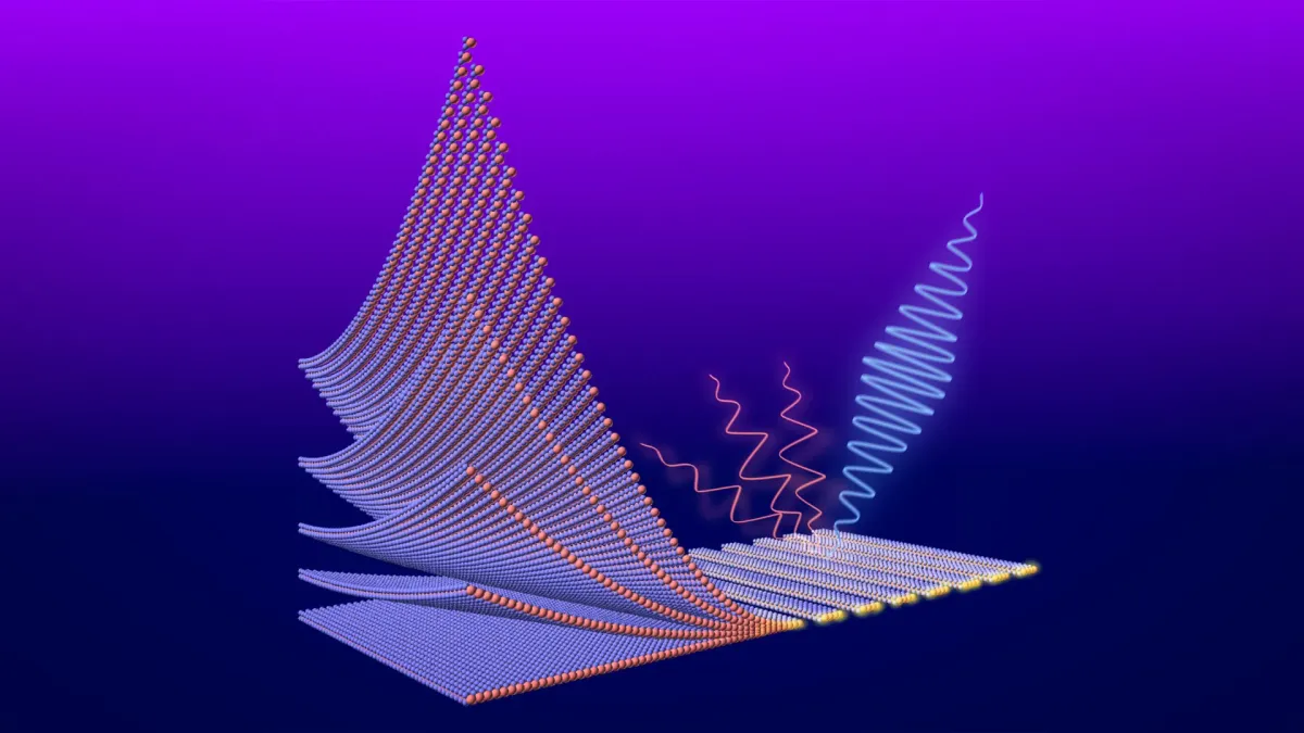
But these researchers built a subwavelength grating with parallel strips so close together, they essentially tricked the infrared light. This grating, made from a special material called molybdenum diselenide (MoSe2), acts like a super-efficient prism, reflecting light almost perfectly while holding it captive in that impossibly thin, 40-nanometer layer.
Why MoSe2? Because it slows light down. A lot. Light slows about 1.5 times in glass and 3.5 times in silicon. In MoSe2? A staggering 4.5 times. This super-slowdown effect means they could make their light trap drastically smaller than with traditional materials like silicon, which would simply let the light escape.
Turning Infrared Into Blue (Because Why Not?)
As if trapping light wasn't enough, MoSe2 has another party trick: it’s a semiconductor with a “nonlinear optical behavior.” In plain English, this means it can take three infrared photons and smash them together to create one higher-frequency photon. The result? You feed it invisible infrared light, and out pops visible blue light. Which, if you think about it, is both impressive and slightly terrifying.
Thanks to the grating’s ability to focus the infrared light so intensely, this conversion is over 1,500 times more efficient than with a flat layer of the same material. Let that satisfying number sink in.
Perhaps even more importantly, they figured out how to make large, uniform films of MoSe2 using molecular beam epitaxy (MBE) — a standard method for growing semiconductors. This means instead of painstakingly peeling off layers with tape (yes, that was a real method), they can now churn out several square inches of this incredibly thin, light-trapping material. Which is good news for anyone hoping to build, say, photonic integrated circuits that fit on the head of a pin.
So, future electronics might not just be smaller and faster; they might be powered by light, controlled by layers thinner than anything you can imagine, and occasionally glow blue. Because the future is apparently both efficient and a little bit magical.