Scientists have figured out how to sculpt materials at the nanoscale in ways that fundamentally change how electricity behaves inside them. A team at Japan's RIKEN Center used a focused ion beam—think of it like a microscopic chisel—to carve helical (spiral) structures from a magnetic crystal. The result: tiny devices that act like switchable diodes, letting current flow easily in one direction while blocking it in the other.
This matters because diodes are everywhere in electronics. They're in your phone's charger (converting AC to DC power), in LED lights, in signal processors. But until now, making them has meant working within the constraints of flat, two-dimensional designs. The new technique opens a different door: what if you could engineer a device's shape itself to control how electricity moves through it.
Shape as a Tool
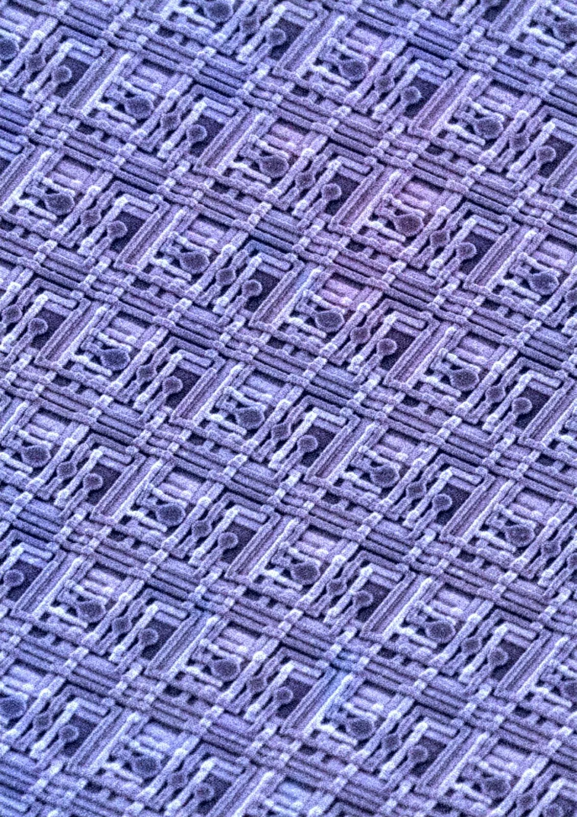
The researchers used cobalt, tin, and sulfur—a material with interesting magnetic properties—and twisted it into helical nanostructures using their ion beam sculpting method. When they tested these spirals, something elegant happened. The twisted geometry created an asymmetry in how electrons scattered along the curved walls, which meant current flowed preferentially in one direction. Flip the magnetic field or reverse the spiral's handedness, and the behavior flipped too. Reversible. Controllable. Precise.
We're a new kind of news feed.
Regular news is designed to drain you. We're a non-profit built to restore you. Every story we publish is scored for impact, progress, and hope.
Start Your News Detox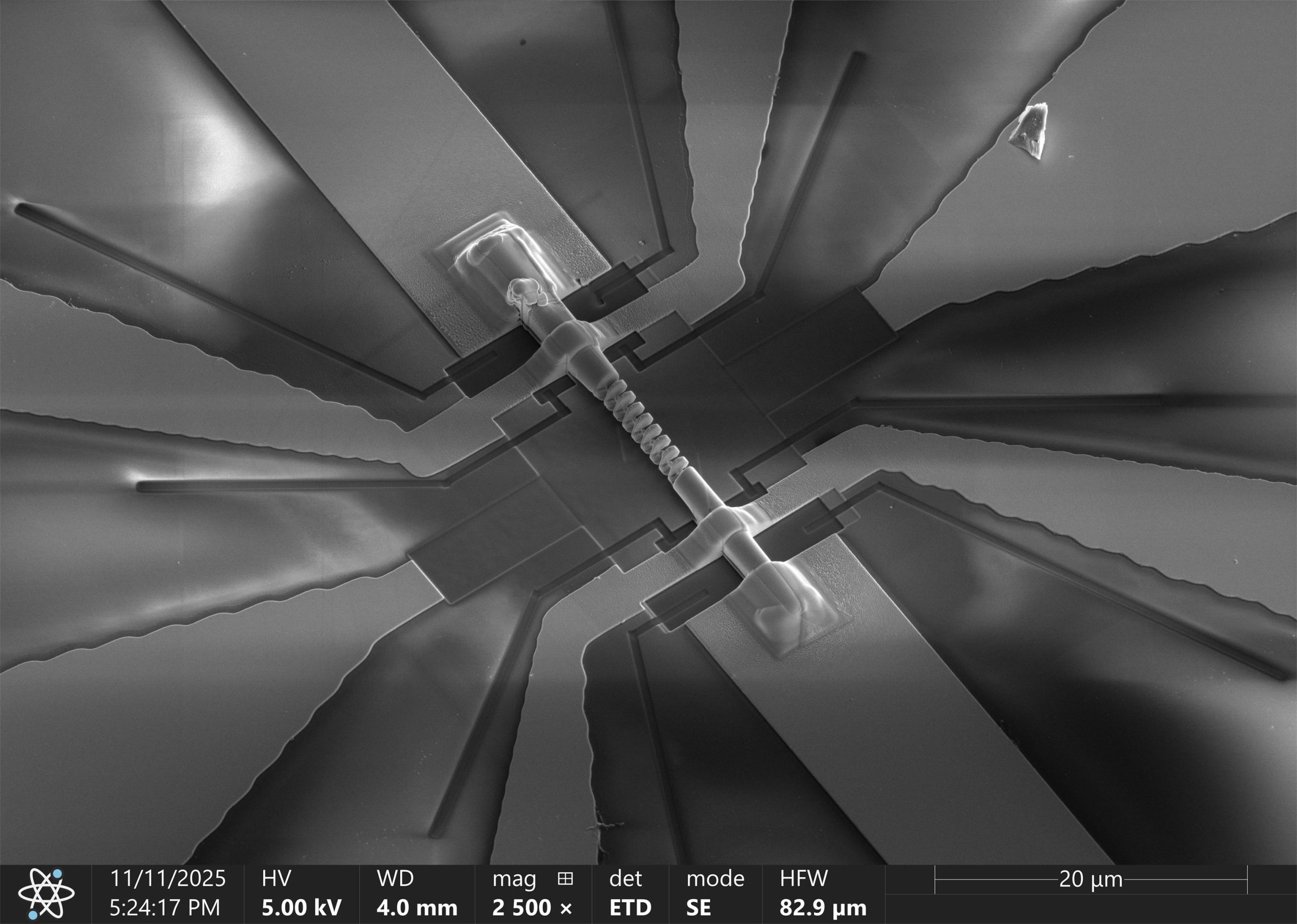
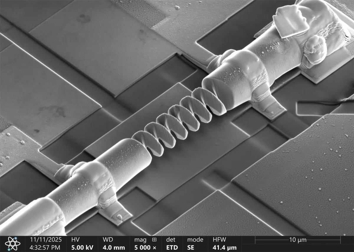
Microscope image of a helical-shaped device crafted using the new method. Credit: RIKEN
What makes this breakthrough significant is the method itself. Previous approaches to building 3D nanostructures were limited—they only worked with certain materials and often damaged the crystal quality in the process. The ion beam technique is different. In principle, it can sculpt almost any crystalline material into almost any 3D shape, much like traditional sculpture but at scales measured in billionths of a meter.
The team's findings, published in Nature Nanotechnology, suggest a shift in how engineers might think about device design. For decades, the focus has been on finding or engineering new materials with special properties. This work shows that the geometry of a component—its shape, its curves, its three-dimensional structure—can be just as important as the material itself. A twisted helix of an ordinary material might do things a flat sheet of an exotic material cannot.
Research leader Yoshinori Tokura noted that this convergence of materials physics and nanofabrication points toward device architectures with potential applications in memory, logic, and sensing technologies. The next steps are likely to involve exploring how other materials and shapes might unlock different electronic behaviors, and whether these principles can scale up from the lab into practical devices.
For now, what's clear is that engineers have a new tool for the toolbox: sculpting at the nanoscale, using shape as a design principle equal to material composition itself.