IBM has unveiled what it calls the world's first sub-1 nanometer semiconductor technology. They built a 0.7 nm chip using a new 3D transistor design. This design aims to push chip scaling beyond today's limits.
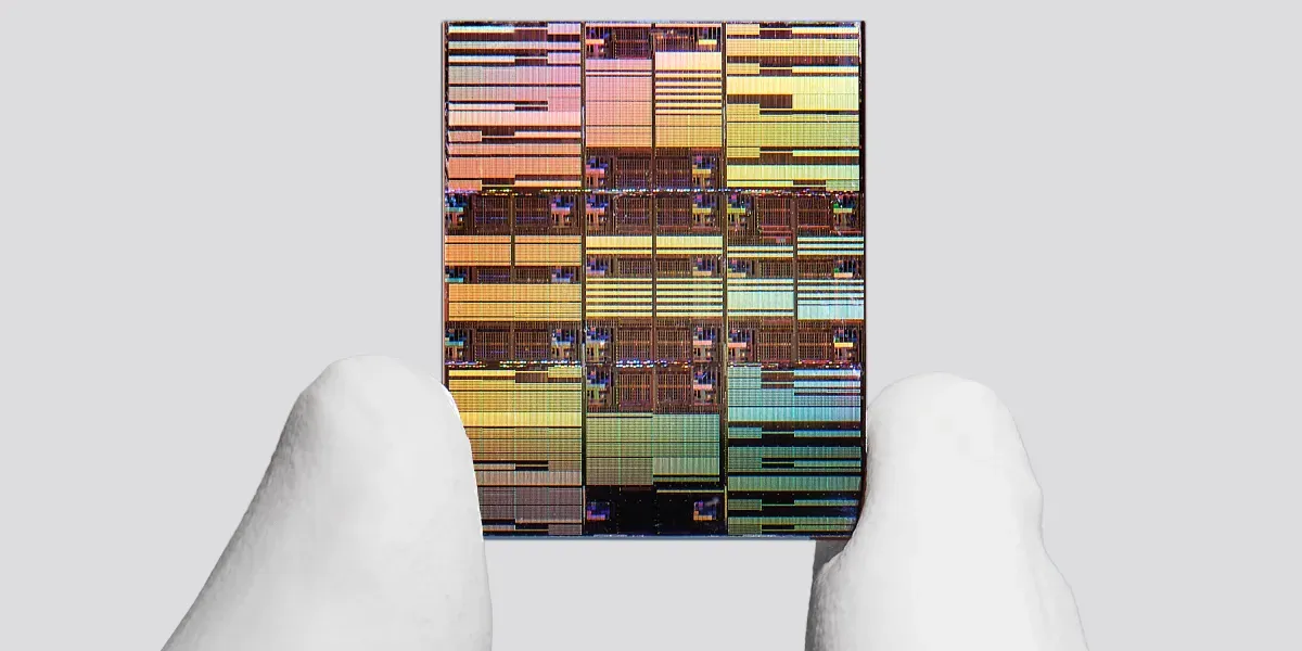
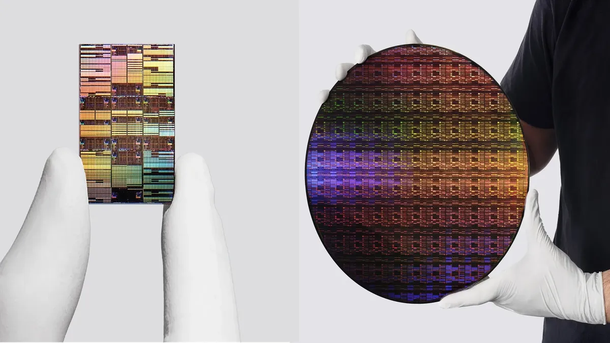
The company stated that this new chip packs nearly 100 billion transistors onto a tiny area, about the size of a fingernail. This nearly doubles the transistor density of IBM's 2 nm chip from 2021.
IBM believes this new technology could offer up to 50% higher performance or 70% better energy efficiency than its 2 nm chips. This could greatly benefit AI systems, cloud computing, and future electronics.
We're a new kind of news feed.
Regular news is designed to drain you. We're a non-profit built to restore you. Every story we publish is scored for impact, progress, and hope.
Start Your News DetoxThis breakthrough comes as the semiconductor industry struggles to make transistors smaller using older designs. IBM says its new architecture allows for continued shrinking, even as chip features get close to atomic sizes.
Beyond Traditional Scaling
The core of this new development is a transistor design called "nanostack." IBM describes it as the first 3D nanosheet-based architecture in the industry.

Unlike typical transistor layouts, nanostack stacks transistors vertically. This allows more components to fit into the same small space. The design also lets engineers use different materials in separate layers. This helps them fine-tune performance and power use independently.
Jay Gambetta, Director of IBM Research, noted that this breakthrough pushes technology beyond the nanometer era to the scale of atoms. He added that nanostack reinvents how chips are built to deliver much more power and energy efficiency.
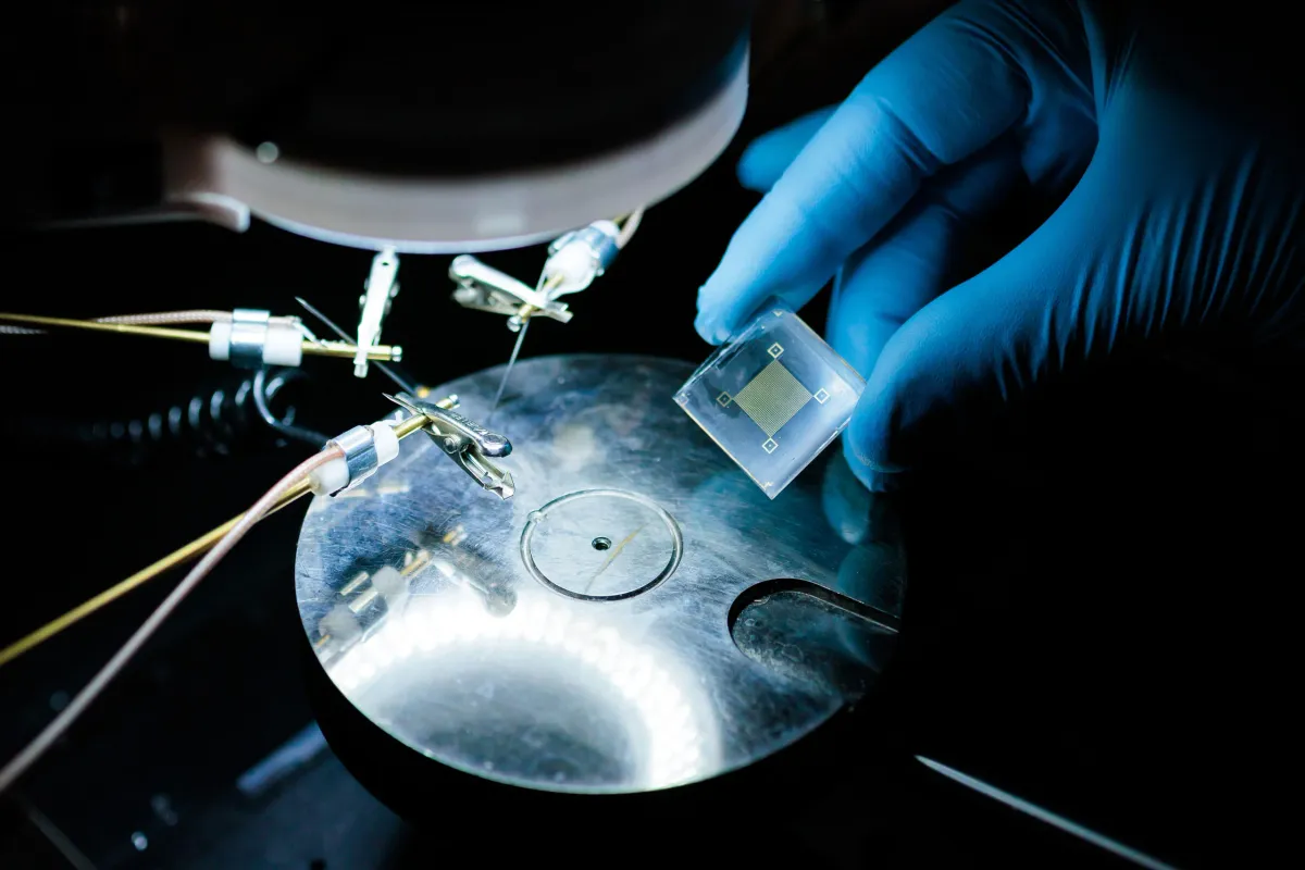
IBM researchers tested the architecture using advanced manufacturing techniques. These tests confirmed that the structure can be made and can perform computing tasks.

The technology also improved memory scaling. IBM reported a 40% reduction in SRAM cell size. This could help chipmakers create denser, more efficient processors. It also supports the growing memory needs of AI workloads.
A Decade-Long Roadmap
IBM thinks the nanostack design could support semiconductor scaling for at least another 10 years.
The company explained that transistor node names no longer mean exact physical sizes. Instead, they identify manufacturing generations. Still, IBM's 0.7 nm (or 7-angstrom) technology shows that further miniaturization is possible below the 1 nm mark.
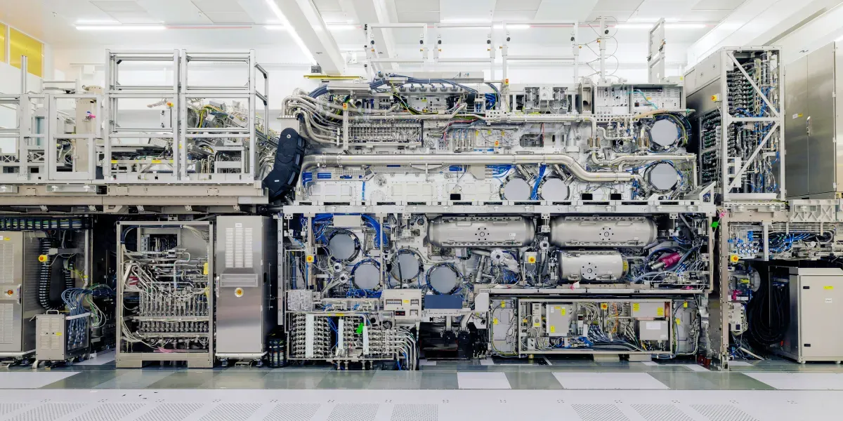
This work is happening at IBM's research facility in Albany, New York. This site will soon have a High Numerical Aperture Extreme Ultraviolet (High NA EUV) lithography system from ASML. This tool is crucial for making future chips.
IBM has been working with Lam Research, Tokyo Electron, and SCREEN Semiconductor Solutions on High NA EUV process development. They have already made working devices using this technology.
IBM expects that nanostack-based chips could be used commercially within the next five years.
The latest findings were shared at the VLSI 2026 Symposium.