A material can look perfect on the outside but still not work right. This often happens because of hidden flaws inside two-dimensional thin films. These films are crucial for the next generation of semiconductor devices. Now, a Korean research team has found a way to spot these invisible defects using light.
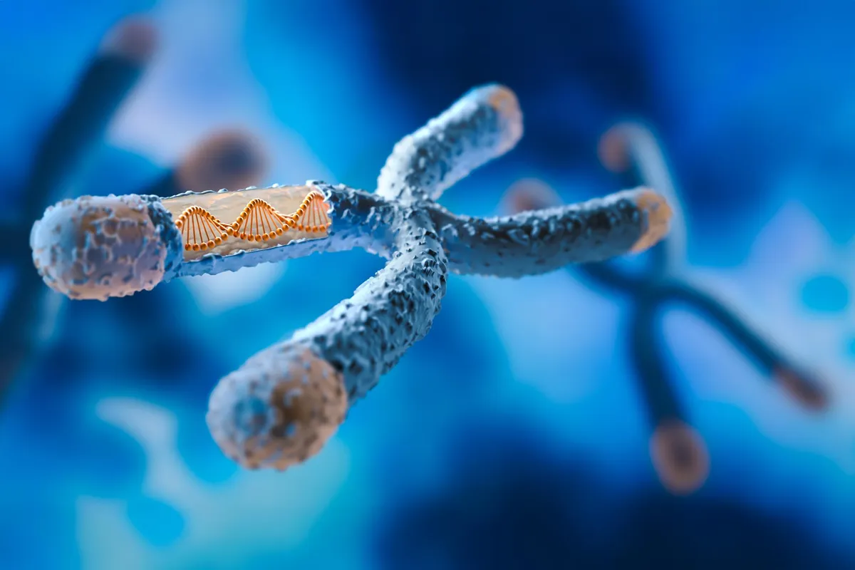
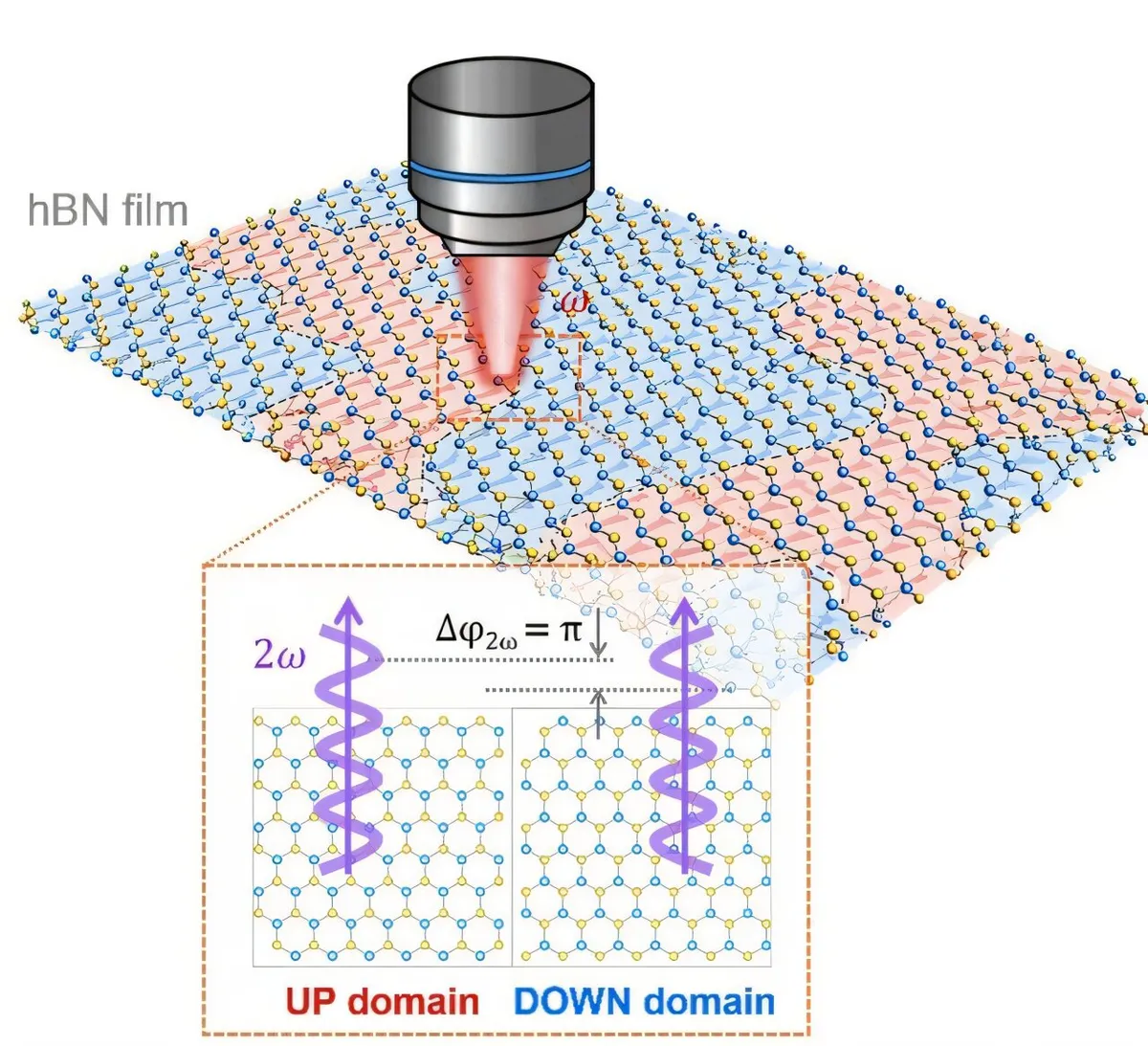
Professor Sunmin Ryu and Ph.D. candidate Yeri Lee from Pohang University of Science and Technology led the team. They developed a method called interferometric second-harmonic generation (SHG) imaging. This technique can optically find hidden structural defects in thin films of hexagonal boron nitride (hBN). hBN is a promising material for future semiconductor technology.
Their findings were published in Advanced Materials.
Finding Hidden Flaws with Light
Two-dimensional materials are becoming essential for new electronic technologies, from smartphones to AI and quantum computers. hBN is especially important. It acts as a "protective layer" for other 2D materials because it's an excellent insulator, preventing electricity from leaking.
We're a new kind of news feed.
Regular news is designed to drain you. We're a non-profit built to restore you. Every story we publish is scored for impact, progress, and hope.
Start Your News DetoxHowever, when hBN is made in large sheets, it can form "antiparallel domains." In these areas, the crystal structures are flipped. Imagine sailors in a boat rowing in opposite directions; these internal signals can clash. This can hurt the material's electrical and optical performance, even if it looks fine.
Traditional methods like transmission electron microscopy (TEM) and scanning tunneling microscopy (STM) are very precise. But they aren't good for quickly checking large areas. Raman spectroscopy is non-destructive but can't directly tell the difference between antiparallel domains.
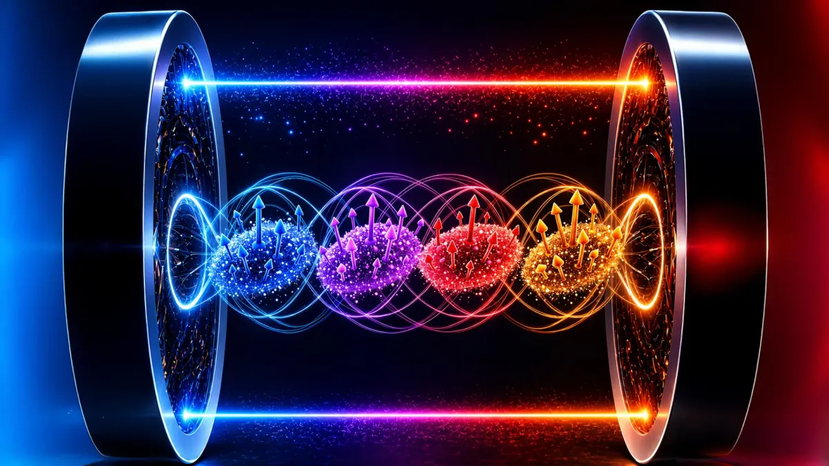
The researchers turned to second-harmonic generation (SHG) imaging to solve these issues. SHG is a special optical effect where light interacting with certain materials creates new light at twice the original frequency.
The team added an external reference signal and carefully analyzed the phase difference between the two signals. They discovered that antiparallel domains have SHG phases that differ by exactly 180 degrees. These domains are common, even in parts of the material that seem to have the same orientation.
They compared 10 hBN thin films grown under different conditions. The team found that changes in SHG intensity are linked to crystal orientation differences. They also saw destructive interference between antiparallel domains. This means that light weakening due to opposing signals can help measure how uneven the crystal structure is.
The team also created optical standards to check the quality and uniformity of hBN. They did this by connecting SHG intensity with Raman spectroscopy data and crystal orientation. This breakthrough doesn't just find one type of defect. It also allows for quick, systematic quality checks of large 2D materials.
Professor Ryu explained that this study shows how antiparallel domains in hBN, which were hard to spot directly, can now be seen optically. He believes this method will be a key tool for improving how 2D materials are grown. It will also help advance future electronic, optical, and quantum devices.
Deep Dive & References
Ubiquitous Antiparallel Domains in 2D Hexagonal Boron Nitride Uncovered by Interferometric Nonlinear Optical Imaging - Advanced Materials, 2026