Researchers at MIT and other institutions have found a new way to make wireless systems faster, more powerful, and use less energy. They did this by embedding gallium nitride (GaN) transistors into a very thin layer of diamond. This diamond layer helps spread heat within the chip.
This method helps keep the chip's temperature even. This allows the transistors to work at their best without becoming unreliable.

Diamond Chips for Better Wireless
Gallium nitride (GaN) is a promising material for advanced wireless uses like 6G and satellite communication. Silicon, which is in most computer chips, has limits on how much power it can handle. GaN can manage higher speeds and energy levels. However, heat has always been a big problem.
We're a new kind of news feed.
Regular news is designed to drain you. We're a non-profit built to restore you. Every story we publish is scored for impact, progress, and hope.
Start Your News DetoxWhen many GaN transistors are packed into small areas on silicon chips, they create hot spots. These hot spots can make the chip less reliable and hurt its performance. The new diamond-based method aims to solve this issue.
Pradyot Yadav, a lead author of the research paper, explained that no single material can do everything well in a wireless device. He noted that these 3D integrated systems are here to stay. Yadav believes that managing heat and ensuring reliability were the main challenges, and this new step could help these systems work at a large scale.

How the Multimaterial Chip Works
This new work builds on systems that combine different materials. In these systems, multiple materials are stacked to use each one's strengths. MIT researchers had previously stacked GaN on silicon and glass to make better chips. But each material can work at a different temperature, which can affect how reliable the chip is.
The researchers used a lab-grown diamond, similar to jewelry-grade diamonds. Diamond is the best known material for conducting heat. Advances in growing single-crystal diamond wafers have made it more practical for use in chips.
Earlier efforts involved growing thin diamond layers on top of GaN transistors. But that process was hard to scale up and could slow down the circuit. Instead, the MIT team embedded tiny GaN transistors, called dielets, into a thin, single-crystal diamond layer.

Yadav said that by putting these GaN transistors into a diamond layer, they actually improved the device's performance instead of making it worse. He added that they get the best of both worlds.
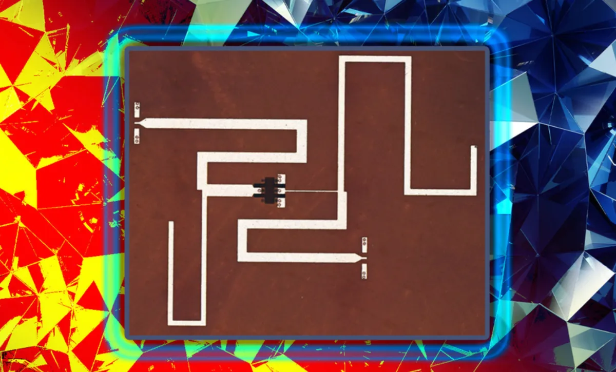
The process starts with a laser cutting GaN dielets from a wafer. Then, the laser drills precise holes into the diamond base. A thin film is placed at the bottom of each hole before the dielet is added.
Setting a New Standard for GaN Chips
The team then stacked layers of insulation and metal on top of the GaN and diamond to create a working circuit. Using this method, they built a power amplifier for wireless communication.
This amplifier showed higher output power, efficiency, and gain than any similar device the researchers found in other studies. This included one they designed themselves in previous work.
These results suggest that the technique could be used for demanding applications. These include high-power radars, space communication, and industrial drones. It could also help manage heat in power conversion systems in data centers, making them more energy-efficient.