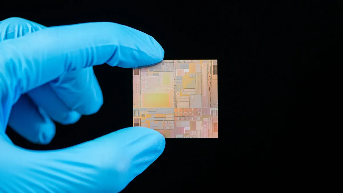
Quantum computers are still in their awkward teenage years — brilliant, but prone to fits of interference. The problem? Tiny, invisible electromagnetic fields lurking on the chips themselves, messing with the delicate quantum calculations.
Enter the super-sleuths at ETH Zurich, who’ve found a way to literally map these hidden fields in 3D, using nothing more than a single, trapped ion. Because apparently, the future of computing depends on making sure your quantum bits aren’t getting static from the chip next door.

The Ultimate Metal Detector for Quantum Noise
Imagine trying to do incredibly precise calculations while someone keeps jiggling the desk. That’s essentially what electrical noise does to quantum chips. Even the weakest electromagnetic disturbances can completely derail a quantum state, making the whole system less accurate. For decades, scientists have been trying to pinpoint these phantom jiggles.
We're a new kind of news feed.
Regular news is designed to drain you. We're a non-profit built to restore you. Every story we publish is scored for impact, progress, and hope.
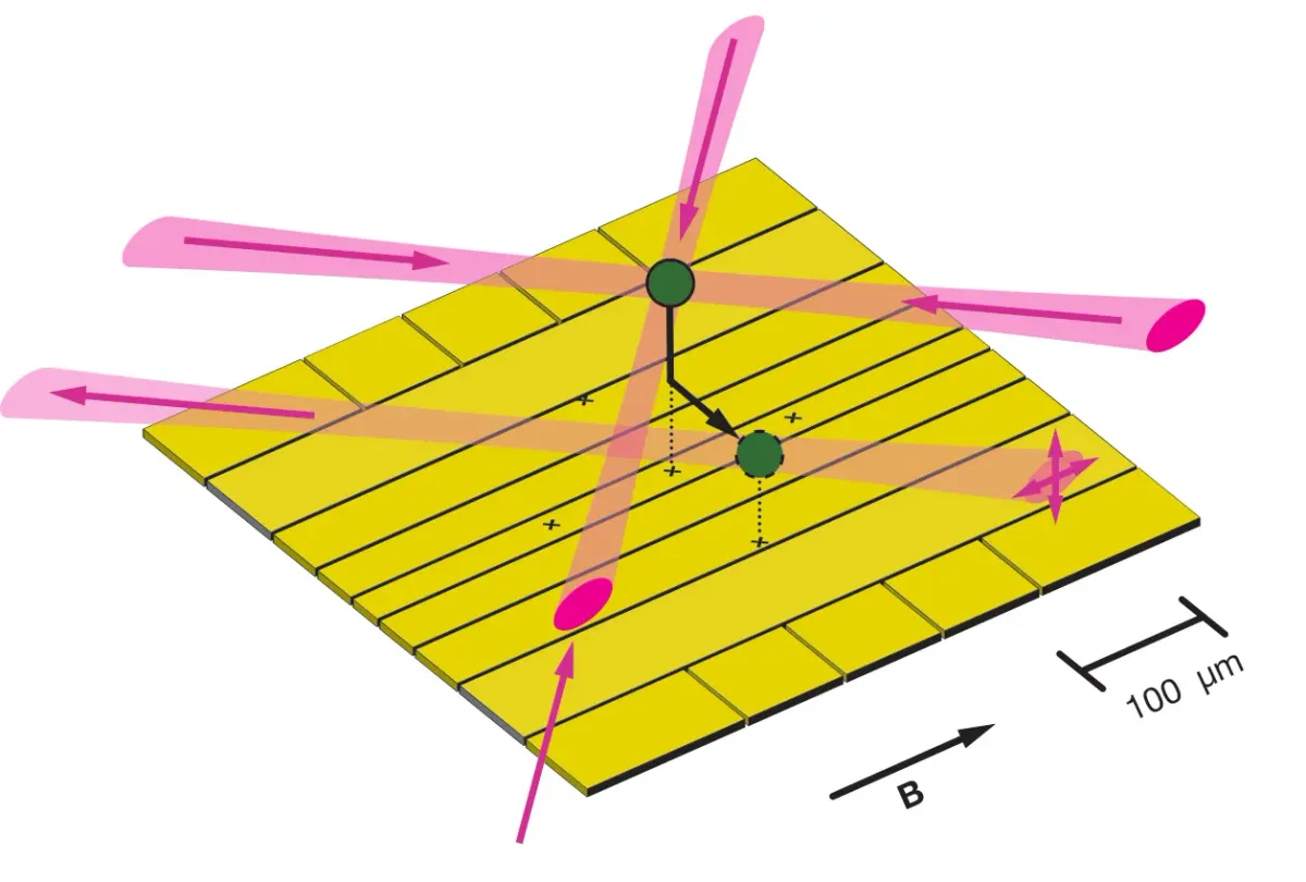
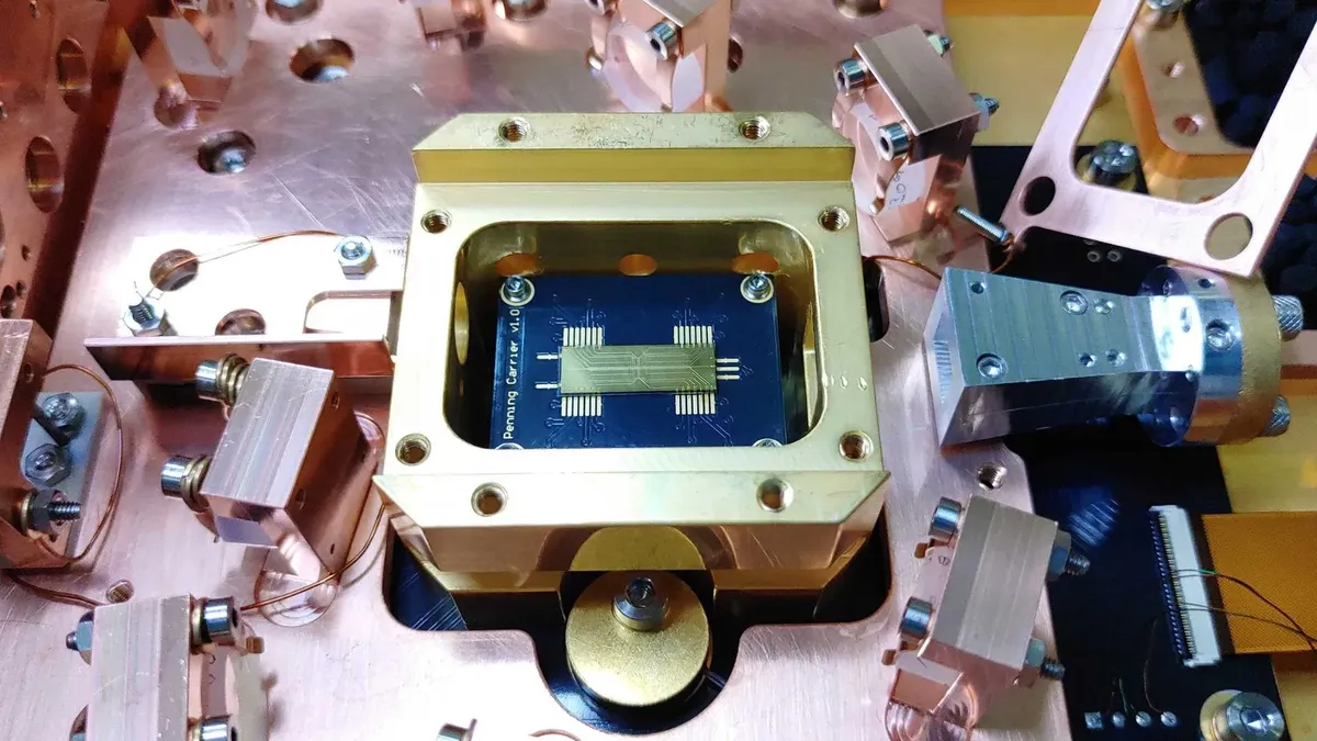
Start Your News DetoxThe ETH Zurich team’s solution involves a chip-based Penning trap, which sounds like something out of a sci-fi novel, but is actually a clever device that holds a single beryllium ion. Unlike other ion traps, this one uses static electric and magnetic fields, allowing the ion to float around freely in three dimensions. Why does that matter? It means they can move the ion wherever they want, turning it into a microscopic scanner.
Doctoral researcher Tobias Sägesser explained that they’d already figured out how to move ions in 3D. Their latest trick is using that ability to scan the space above a chip, creating a detailed electromagnetic field map. Think of it as an MRI for your quantum hardware.
Sensing the Unseeable
The process is delightfully intricate: First, they cool a single beryllium ion with lasers until it’s practically frozen in its lowest quantum motion state. Then, they nudge it to different spots above the chip by tweaking voltages on the trap electrodes. It can scan an area about the size of a dust mite (200 by 200 micrometers) and heights ranging from 50 to 450 micrometers above the surface.
At each tiny point, if there’s a weak electric field from the chip, it subtly increases the ion’s motion. They then zap it with laser pulses to see how much its quantum state has changed, which tells them the strength of the surrounding electric field. It’s like using a super-sensitive quantum seismograph.
Sägesser noted they made the most sensitive measurement yet of an oscillating electric field inside a chip trap, detecting a signal of just 10 nanovolts per meter in one second. For context, the electromagnetic field from your cellphone is about 10,000 times stronger, even if it’s several kilometers away. Let that satisfying number sink in.
They also measured static electric fields by observing how stray fields gently pushed the ion from its resting position. Magnetic fields? Those were found by tracking shifts in the ion’s energy levels. It’s a full-spectrum analysis.
Professor Jonathan Home, who’s been in this game for over 30 years, says this new method gives them precise 3D measurements they can directly compare with theoretical models. This makes it far easier to pinpoint exactly where the interference is coming from. The Penning trap even allows them to temporarily disconnect it from outside power, reducing external noise that used to make these experiments a nightmare.
Ultimately, this technique will be crucial for testing different materials, surface coatings, and manufacturing methods for quantum chips. The goal? To find the combinations that create the least electrical noise, paving the way for quantum computers and sensors that actually work as advertised. Because if we’re going to build a quantum future, we might as well make sure it’s a quiet one.